
Klein, Amelia R.; Engheta, Nader; Bassett, Lee C.
Designing metasurface optical interfaces for solid-state qubits using many-body adjoint shape optimization Journal Article
In: Optics Express, vol. 32, iss. 22, pp. 38504-38515, 2024.
Abstract | Links | BibTeX | Tags: diamond fabrication, diamond NV center, Nanophotonics, photoluminescence
@article{Klein2024,
title = {Designing metasurface optical interfaces for solid-state qubits using many-body adjoint shape optimization},
author = {Amelia R. Klein and Nader Engheta and Lee C. Bassett},
url = {https://opg.optica.org/oe/fulltext.cfm?uri=oe-32-22-38504&id=561330
https://arxiv.org/abs/2406.08212},
doi = {10.1364/OE.522501},
year = {2024},
date = {2024-10-09},
urldate = {2024-10-09},
journal = {Optics Express},
volume = {32},
issue = {22},
pages = {38504-38515},
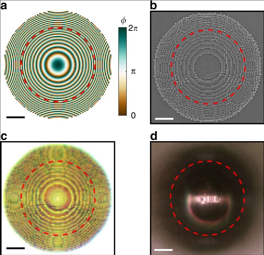
abstract = {We present a general strategy for the inverse design of metasurfaces composed of elementary shapes. We use it to design a structure that collects and collimates light from nitrogen-vacancy centers in diamond. Such metasurfaces constitute scalable optical interfaces for solid-state qubits, enabling efficient photon coupling into optical fibers and eliminating free-space collection optics. The many-body shape optimization strategy is a practical alternative to topology optimization that explicitly enforces material and fabrication constraints throughout the optimization, while still achieving high performance. The metasurface is easily adaptable to other solid-state qubits, and the optimization method is broadly applicable to fabrication-constrained photonic design problems.},
keywords = {diamond fabrication, diamond NV center, Nanophotonics, photoluminescence},
pubstate = {published},
tppubtype = {article}
}
Shulevitz, Henry J.; Huang, Tzu-Yung; Xu, Jun; Neuhaus, Steven; Patel, Raj N.; Lee C. Bassett, Cherie R. Kagan
Template-Assisted Self Assembly of Fluorescent Nanodiamonds for Scalable Quantum Technologies Journal Article
In: ACS Nano, vol. 16, no. 2, pp. 1847–1856, 2022.
Abstract | Links | BibTeX | Tags: Condensed Matter, diamond NV center, nanodiamond assembly, Nanophotonics
@article{Shulevitz2021,
title = {Template-Assisted Self Assembly of Fluorescent Nanodiamonds for Scalable Quantum Technologies},
author = {Henry J. Shulevitz and Tzu-Yung Huang and Jun Xu and Steven Neuhaus and Raj N. Patel and Lee C. Bassett, Cherie R. Kagan},
url = {https://arxiv.org/abs/2111.14921},
doi = {10.1021/acsnano.1c09839},
year = {2022},
date = {2022-01-13},
journal = {ACS Nano},
volume = {16},
number = {2},
pages = {1847–1856},
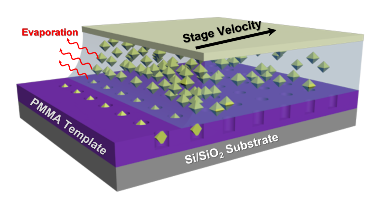
abstract = {Milled nanodiamonds containing nitrogen-vacancy (NV) centers provide an excellent platform for sensing applications as they are optically robust, have nanoscale quantum sensitivity, and form colloidal dispersions which enable bottom-up assembly techniques for device integration. However, variations in their size, shape, and surface chemistry limit the ability to position individual nanodiamonds and statistically study properties that affect their optical and quantum characteristics. Here, we present a scalable strategy to form ordered arrays of nanodiamonds using capillary-driven, template-assisted self assembly. This method enables the precise spatial arrangement of isolated nanodiamonds with diameters below 50 nm across millimeter-scale areas. Measurements of over 200 assembled nanodiamonds yield a statistical understanding of their structural, optical, and quantum properties. The NV centers' spin and charge properties are uncorrelated with nanodiamond size, but rather are consistent with heterogeneity in their nanoscale environment. This flexible assembly method, together with improved understanding of the material, will enable the integration of nanodiamonds into future quantum photonic and electronic devices.},
keywords = {Condensed Matter, diamond NV center, nanodiamond assembly, Nanophotonics},
pubstate = {published},
tppubtype = {article}
}
Bassett, L. C.; Alkauskas, A.; Exarhos, A. L.; Fu, K. -M. C.
Quantum defects by design Journal Article
In: Nanophotonics, vol. 8, no. 11, 2019.
Abstract | Links | BibTeX | Tags: Nanophotonics, optical sources, point defects, Quantum Control
@article{Bassett2019b,
title = {Quantum defects by design},
author = {L. C. Bassett and A. Alkauskas and A. L. Exarhos and K.-M. C. Fu},
url = {https://www.degruyter.com/view/journals/nanoph/8/11/article-p1867.xml},
year = {2019},
date = {2019-10-04},
journal = {Nanophotonics},
volume = {8},
number = {11},
abstract = {Part of Special Issue on Quantum Nanophotonics in Emerging Materials.
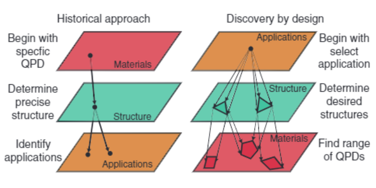
Miniaturization of electronic and opto-electronic semiconductor devices has been happening ever since the first such devices appeared. Eventually, one can envision a device that is composed of just a few atoms. As these atoms ideally should not float in free space, but should be embedded in a solid-state matrix, this naturally brings one to the concept of a point defect (an impurity atom or complex of atoms) as the ultimate electronic or opto-electronic device. At such tiny length scales the behavior of physical systems is governed by the laws of quantum mechanics. Therefore, it is no surprise that an increasing number of point defects are being considered as building blocks for various applications in the field of quantum information science; more specifically, in quantum sensing, quantum communication, and quantum computing [1], [2], [3], [4]. We refer to these desirable defects as quantum point defects (QPDs). Prominent examples include the nitrogen-vacancy (NV) center in diamond, the silicon-vacancy (SiV) center in diamond, the divacancy in silicon carbide, and rare-earth impurities in complex oxides.},
keywords = {Nanophotonics, optical sources, point defects, Quantum Control},
pubstate = {published},
tppubtype = {article}
}
Miniaturization of electronic and opto-electronic semiconductor devices has been happening ever since the first such devices appeared. Eventually, one can envision a device that is composed of just a few atoms. As these atoms ideally should not float in free space, but should be embedded in a solid-state matrix, this naturally brings one to the concept of a point defect (an impurity atom or complex of atoms) as the ultimate electronic or opto-electronic device. At such tiny length scales the behavior of physical systems is governed by the laws of quantum mechanics. Therefore, it is no surprise that an increasing number of point defects are being considered as building blocks for various applications in the field of quantum information science; more specifically, in quantum sensing, quantum communication, and quantum computing [1], [2], [3], [4]. We refer to these desirable defects as quantum point defects (QPDs). Prominent examples include the nitrogen-vacancy (NV) center in diamond, the silicon-vacancy (SiV) center in diamond, the divacancy in silicon carbide, and rare-earth impurities in complex oxides.
Huang, T -Y; Grote, R R; Mann, S A; Hopper, D A; Exarhos, A L; Lopez, G G; Klein, A R; Garnett, E C; Bassett, L C
Imaging a nitrogen-vacancy center with a diamond immersion metalens Journal Article
In: Nature Communications, vol. 10, no. 2392, 2019.
Abstract | Links | BibTeX | Tags: diamond fabrication, Nanophotonics
@article{Huang2019,
title = {Imaging a nitrogen-vacancy center with a diamond immersion metalens},
author = {T -Y Huang and R R Grote and S A Mann and D A Hopper and A L Exarhos and G G Lopez and A R Klein and E C Garnett and L C Bassett},
url = {https://www.nature.com/articles/s41467-019-10238-5
https://medium.com/penn-engineering/penn-engineers-design-nanostructured-diamond-metalens-for-compact-quantum-technologies-271adddf69ba},
year = {2019},
date = {2019-06-03},
journal = {Nature Communications},
volume = {10},
number = {2392},
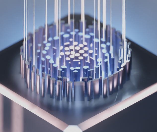
abstract = {Quantum emitters such as the diamond nitrogen-vacancy (NV) center are the basis for a wide range of quantum technologies. However, refraction and reflections at material interfaces impede photon collection, and the emitters’ atomic scale necessitates the use of free space optical measurement setups that prevent packaging of quantum devices. To overcome these limitations, we design and fabricate a metasurface composed of nanoscale diamond pillars that acts as an immersion lens to collect and collimate the emission of an individual NV center. The metalens exhibits a numerical aperture greater than 1.0, enabling efficient fiber-coupling of quantum emitters. This flexible design will lead to the miniaturization of quantum devices in a wide range of host materials and the development of metasurfaces that shape single-photon emission for coupling to optical cavities or route photons based on their quantum state.},
keywords = {diamond fabrication, Nanophotonics},
pubstate = {published},
tppubtype = {article}
}
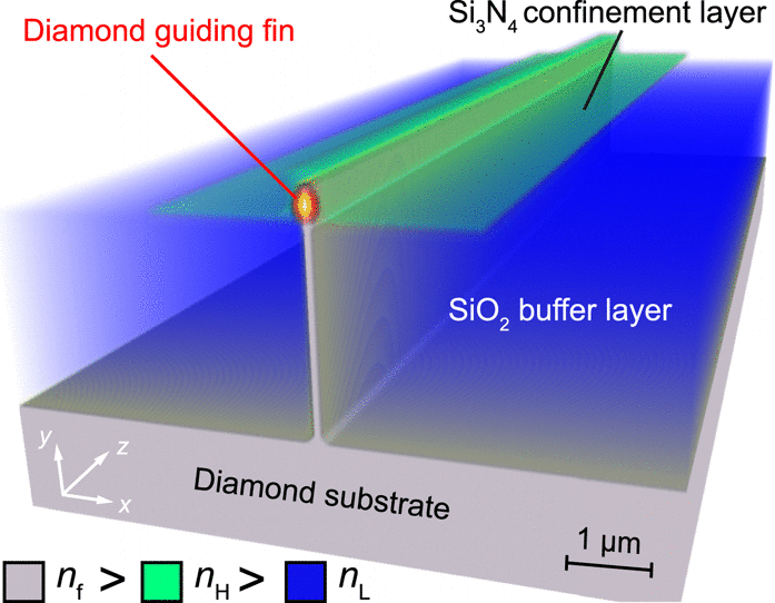
Grote, R R; Bassett, L C
Single-mode optical waveguides on native high-refractive-index substrates Journal Article
In: APL Photonics, vol. 1, pp. 071302, 2016.
Abstract | Links | BibTeX | Tags: diamond fabrication, Nanophotonics
@article{Grote2016,

title = {Single-mode optical waveguides on native high-refractive-index substrates},

author = {R R Grote and L C Bassett},

url = {https://aip.scitation.org/doi/10.1063/1.4955065},

year  = {2016},

date = {2016-08-01},

journal = {APL Photonics},

volume = {1},

pages = {071302},

abstract = {High-refractive-index semiconductor optical waveguides form the basis for modern photonic integrated circuits (PICs). However, conventional methods for achieving optical confinement require a thick lower-refractive-index support layer that impedes large-scale co-integration with electronics and limits the materials on which PICs can be fabricated. To address this challenge, we present a general architecture for single-mode waveguides that confine light in a high-refractive-index material on a native substrate. The waveguide consists of a high-aspect-ratio fin of the guiding material surrounded by lower-refractive-index dielectrics and is compatible with standard top-down fabrication techniques. This letter describes a physically intuitive, semi-analytical, effective index model for designing fin waveguides, which is confirmed with fully vectorial numerical simulations. Design examples are presented for diamond and silicon at visible and telecommunications wavelengths, respectively, along with calculations of propagation loss due to bending, scattering, and substrate leakage. Potential methods of fabrication are also discussed. The proposed waveguide geometry allows PICs to be fabricated alongside silicon CMOS electronics on the same wafer, removes the need for heteroepitaxy in III-V PICs, and will enable wafer-scale photonic integration on emerging material platforms such as diamond and SiC.},

keywords = {diamond fabrication, Nanophotonics},

pubstate = {published},

tppubtype = {article}

}
2024
Klein, Amelia R.; Engheta, Nader; Bassett, Lee C.
Designing metasurface optical interfaces for solid-state qubits using many-body adjoint shape optimization Journal Article
In: Optics Express, vol. 32, iss. 22, pp. 38504-38515, 2024.
@article{Klein2024,

title = {Designing metasurface optical interfaces for solid-state qubits using many-body adjoint shape optimization},

author = {Amelia R. Klein and Nader Engheta and Lee C. Bassett},

url = {https://opg.optica.org/oe/fulltext.cfm?uri=oe-32-22-38504&id=561330

https://arxiv.org/abs/2406.08212},

doi = {10.1364/OE.522501},

year  = {2024},

date = {2024-10-09},

urldate = {2024-10-09},

journal = {Optics Express},

volume = {32},

issue = {22},

pages = {38504-38515},

abstract = {We present a general strategy for the inverse design of metasurfaces composed of elementary shapes. We use it to design a structure that collects and collimates light from nitrogen-vacancy centers in diamond. Such metasurfaces constitute scalable optical interfaces for solid-state qubits, enabling efficient photon coupling into optical fibers and eliminating free-space collection optics. The many-body shape optimization strategy is a practical alternative to topology optimization that explicitly enforces material and fabrication constraints throughout the optimization, while still achieving high performance. The metasurface is easily adaptable to other solid-state qubits, and the optimization method is broadly applicable to fabrication-constrained photonic design problems.},

keywords = {},

pubstate = {published},

tppubtype = {article}

}
2022
Shulevitz, Henry J.; Huang, Tzu-Yung; Xu, Jun; Neuhaus, Steven; Patel, Raj N.; Lee C. Bassett, Cherie R. Kagan
Template-Assisted Self Assembly of Fluorescent Nanodiamonds for Scalable Quantum Technologies Journal Article
In: ACS Nano, vol. 16, no. 2, pp. 1847–1856, 2022.
@article{Shulevitz2021,

title = {Template-Assisted Self Assembly of Fluorescent Nanodiamonds for Scalable Quantum Technologies},

author = {Henry J. Shulevitz and Tzu-Yung Huang and Jun Xu and Steven Neuhaus and Raj N. Patel and Lee C. Bassett, Cherie R. Kagan},

url = {https://arxiv.org/abs/2111.14921},

doi = {10.1021/acsnano.1c09839},

year  = {2022},

date = {2022-01-13},

journal = {ACS Nano},

volume = {16},

number = {2},

pages = {1847–1856},

abstract = {Milled nanodiamonds containing nitrogen-vacancy (NV) centers provide an excellent platform for sensing applications as they are optically robust, have nanoscale quantum sensitivity, and form colloidal dispersions which enable bottom-up assembly techniques for device integration. However, variations in their size, shape, and surface chemistry limit the ability to position individual nanodiamonds and statistically study properties that affect their optical and quantum characteristics. Here, we present a scalable strategy to form ordered arrays of nanodiamonds using capillary-driven, template-assisted self assembly. This method enables the precise spatial arrangement of isolated nanodiamonds with diameters below 50 nm across millimeter-scale areas. Measurements of over 200 assembled nanodiamonds yield a statistical understanding of their structural, optical, and quantum properties. The NV centers' spin and charge properties are uncorrelated with nanodiamond size, but rather are consistent with heterogeneity in their nanoscale environment. This flexible assembly method, together with improved understanding of the material, will enable the integration of nanodiamonds into future quantum photonic and electronic devices.},

keywords = {},

pubstate = {published},

tppubtype = {article}

}
2019
Bassett, L. C.; Alkauskas, A.; Exarhos, A. L.; Fu, K. -M. C.
Quantum defects by design Journal Article
In: Nanophotonics, vol. 8, no. 11, 2019.
@article{Bassett2019b,

title = {Quantum defects by design},

author = {L. C. Bassett and A. Alkauskas and A. L. Exarhos and K.-M. C. Fu},

url = {https://www.degruyter.com/view/journals/nanoph/8/11/article-p1867.xml},

year  = {2019},

date = {2019-10-04},

journal = {Nanophotonics},

volume = {8},

number = {11},

abstract = {Part of Special Issue on Quantum Nanophotonics in Emerging Materials.


Miniaturization of electronic and opto-electronic semiconductor devices has been happening ever since the first such devices appeared. Eventually, one can envision a device that is composed of just a few atoms. As these atoms ideally should not float in free space, but should be embedded in a solid-state matrix, this naturally brings one to the concept of a point defect (an impurity atom or complex of atoms) as the ultimate electronic or opto-electronic device. At such tiny length scales the behavior of physical systems is governed by the laws of quantum mechanics. Therefore, it is no surprise that an increasing number of point defects are being considered as building blocks for various applications in the field of quantum information science; more specifically, in quantum sensing, quantum communication, and quantum computing [1], [2], [3], [4]. We refer to these desirable defects as quantum point defects (QPDs). Prominent examples include the nitrogen-vacancy (NV) center in diamond, the silicon-vacancy (SiV) center in diamond, the divacancy in silicon carbide, and rare-earth impurities in complex oxides.},

keywords = {},

pubstate = {published},

tppubtype = {article}

}
Miniaturization of electronic and opto-electronic semiconductor devices has been happening ever since the first such devices appeared. Eventually, one can envision a device that is composed of just a few atoms. As these atoms ideally should not float in free space, but should be embedded in a solid-state matrix, this naturally brings one to the concept of a point defect (an impurity atom or complex of atoms) as the ultimate electronic or opto-electronic device. At such tiny length scales the behavior of physical systems is governed by the laws of quantum mechanics. Therefore, it is no surprise that an increasing number of point defects are being considered as building blocks for various applications in the field of quantum information science; more specifically, in quantum sensing, quantum communication, and quantum computing [1], [2], [3], [4]. We refer to these desirable defects as quantum point defects (QPDs). Prominent examples include the nitrogen-vacancy (NV) center in diamond, the silicon-vacancy (SiV) center in diamond, the divacancy in silicon carbide, and rare-earth impurities in complex oxides.
Huang, T -Y; Grote, R R; Mann, S A; Hopper, D A; Exarhos, A L; Lopez, G G; Klein, A R; Garnett, E C; Bassett, L C
Imaging a nitrogen-vacancy center with a diamond immersion metalens Journal Article
In: Nature Communications, vol. 10, no. 2392, 2019.
@article{Huang2019,

title = {Imaging a nitrogen-vacancy center with a diamond immersion metalens},

author = {T -Y Huang and R R Grote and S A Mann and D A Hopper and A L Exarhos and G G Lopez and A R Klein and E C Garnett and L C Bassett},

url = {https://www.nature.com/articles/s41467-019-10238-5

https://medium.com/penn-engineering/penn-engineers-design-nanostructured-diamond-metalens-for-compact-quantum-technologies-271adddf69ba},

year  = {2019},

date = {2019-06-03},

journal = {Nature Communications},

volume = {10},

number = {2392},

abstract = {Quantum emitters such as the diamond nitrogen-vacancy (NV) center are the basis for a wide range of quantum technologies. However, refraction and reflections at material interfaces impede photon collection, and the emitters’ atomic scale necessitates the use of free space optical measurement setups that prevent packaging of quantum devices. To overcome these limitations, we design and fabricate a metasurface composed of nanoscale diamond pillars that acts as an immersion lens to collect and collimate the emission of an individual NV center. The metalens exhibits a numerical aperture greater than 1.0, enabling efficient fiber-coupling of quantum emitters. This flexible design will lead to the miniaturization of quantum devices in a wide range of host materials and the development of metasurfaces that shape single-photon emission for coupling to optical cavities or route photons based on their quantum state.},

keywords = {},

pubstate = {published},

tppubtype = {article}

}
2016
Grote, R R; Bassett, L C
Single-mode optical waveguides on native high-refractive-index substrates Journal Article
In: APL Photonics, vol. 1, pp. 071302, 2016.
@article{Grote2016,

title = {Single-mode optical waveguides on native high-refractive-index substrates},

author = {R R Grote and L C Bassett},

url = {https://aip.scitation.org/doi/10.1063/1.4955065},

year  = {2016},

date = {2016-08-01},

journal = {APL Photonics},

volume = {1},

pages = {071302},

abstract = {High-refractive-index semiconductor optical waveguides form the basis for modern photonic integrated circuits (PICs). However, conventional methods for achieving optical confinement require a thick lower-refractive-index support layer that impedes large-scale co-integration with electronics and limits the materials on which PICs can be fabricated. To address this challenge, we present a general architecture for single-mode waveguides that confine light in a high-refractive-index material on a native substrate. The waveguide consists of a high-aspect-ratio fin of the guiding material surrounded by lower-refractive-index dielectrics and is compatible with standard top-down fabrication techniques. This letter describes a physically intuitive, semi-analytical, effective index model for designing fin waveguides, which is confirmed with fully vectorial numerical simulations. Design examples are presented for diamond and silicon at visible and telecommunications wavelengths, respectively, along with calculations of propagation loss due to bending, scattering, and substrate leakage. Potential methods of fabrication are also discussed. The proposed waveguide geometry allows PICs to be fabricated alongside silicon CMOS electronics on the same wafer, removes the need for heteroepitaxy in III-V PICs, and will enable wafer-scale photonic integration on emerging material platforms such as diamond and SiC.},

keywords = {},

pubstate = {published},

tppubtype = {article}

}
Select publications before 2014
- “All-optical control of a solid-state spin using coherent dark states”, C. G. Yale, B. B. Buckley, D. J. Christle, G. Burkard, F. J. Heremans, L. C. Bassett, and D. D. Awschalom, Proc. Natl. Acad. Sci. USA 110, 7595 (2013).
- “Quantum spintronics: Engineering and manipulating atom-like spins in semiconductors”, D.D. Awschalom, L.C. Bassett, A.S. Dzurak, E.L. Hu and J.R. Petta, Science 339, 1174 (2013).
Related article: “The Future of Quantum Information Processing”, J. Stajic, Science 339, 1163 (2013).
- “Engineering and quantum control of single spins in semiconductors”, D.M. Toyli, L.C. Bassett, B.B. Buckley, G. Calusine and D.D. Awschalom, MRS Bulletin 38, 139 (2013).
- “Engineering shallow spins in diamond with nitrogen delta-doping”, K. Ohno, F. J. Heremans, L. C. Bassett, B. A. Myers, D. M. Toyli, A. C. Bleszynski-Jayich, C. J. Palmstrøm, and D. D. Awschalom, Appl. Phys. Lett. 101, 082413 (2012).
- “Electrical tuning of single nitrogen-vacancy center optical transitions enhanced by photoinduced fields”, L. C. Bassett, F. J. Heremans, C. G. Yale, B. B. Buckley, and D. D. Awschalom, Phys. Rev. Lett. 107, 266403 (2011).
- “Spin-light coherence for single-spin measurement and control in diamond”, B. B. Buckley, G. D. Fuchs, L. C. Bassett, and D. D. Awschalom, Science 330, 1212 (2010).
Related article: “Quantum measurement and control of single spins in diamond”, Science 330, 1188 (2010).