
Breitweiser, S. Alex; Ouellet, Mathieu; Huang, Tzu-Yung; Taminiau, Tim H.; Bassett, Lee C.
Quadrupolar resonance spectroscopy of individual nuclei using a room-temperature quantum sensor Journal Article
In: Nano Letters, vol. 24, iss. 51, pp. 16253-16260, 2024.
Abstract | Links | BibTeX | Tags: diamond NV center, NQR spectroscopy, point defects, quantum sensing
@article{Breitweiser2024,
title = {Quadrupolar resonance spectroscopy of individual nuclei using a room-temperature quantum sensor},
author = {S. Alex Breitweiser and Mathieu Ouellet and Tzu-Yung Huang and Tim H. Taminiau and Lee C. Bassett},
url = {https://pubs.acs.org/doi/abs/10.1021/acs.nanolett.4c04112
https://arxiv.org/abs/2405.14859},
year = {2024},
date = {2024-12-12},
urldate = {2024-12-12},
journal = {Nano Letters},
volume = {24},
issue = {51},
pages = {16253-16260},
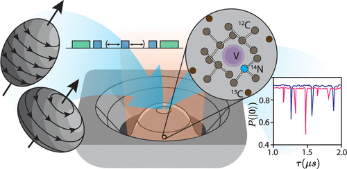
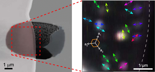
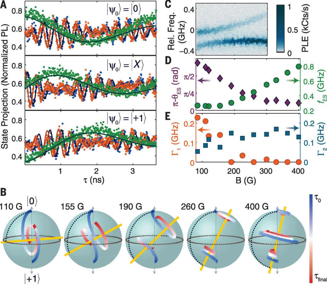
abstract = {Nuclear quadrupolar resonance (NQR) spectroscopy reveals chemical bonding patterns in materials and molecules through the unique coupling between nuclear spins and local fields. However, traditional NQR techniques require macroscopic ensembles of nuclei to yield a detectable signal, which obscures molecule-to-molecule variations. Solid-state spin qubits, such as the nitrogen-vacancy (NV) center in diamond, facilitate the detection and control of individual nuclei through their local magnetic couplings. Here, we use NV centers to perform NQR spectroscopy on their associated nitrogen-14 (14N) nuclei at room temperature. In mapping the nuclear quadrupolar Hamiltonian, we resolve minute variations between individual nuclei. The measurements reveal correlations between the Hamiltonian parameters associated with the NV center’s electronic and nuclear spin states, as well as a previously unreported symmetry-breaking quadrupolar term. We further design pulse sequences to initialize, read out, and control the quantum evolution of the 14N nuclear state using the nuclear quadrupolar Hamiltonian.},
keywords = {diamond NV center, NQR spectroscopy, point defects, quantum sensing},
pubstate = {published},
tppubtype = {article}
}
Patel, Raj N.; Fishman, Rebecca E. K.; Huang, Tzu-Yung; Gusdorff, Jordan A.; Fehr, David A.; Hopper, David A.; Breitweiser, S. Alex; Porat, Benjamin; Flatté, Michael E.; Bassett, Lee C.
Room Temperature Dynamics of an Optically Addressable Single Spin in Hexagonal Boron Nitride Journal Article
In: Nano Letters, vol. 24, iss. 25, pp. 7623-7628, 2024.
Abstract | Links | BibTeX | Tags: 2-dimensional systems, First-principles calculations, photon emission correlation spectroscopy, photon statistics, point defects
@article{Patel2024,
title = {Room Temperature Dynamics of an Optically Addressable Single Spin in Hexagonal Boron Nitride},
author = {Raj N. Patel and Rebecca E. K. Fishman and Tzu-Yung Huang and Jordan A. Gusdorff and David A. Fehr and David A. Hopper and S. Alex Breitweiser and Benjamin Porat and Michael E. Flatté and Lee C. Bassett},
url = {https://pubs.acs.org/doi/abs/10.1021/acs.nanolett.4c01333
https://arxiv.org/abs/2309.05604},
doi = {10.1021/acs.nanolett.4c01333},
year = {2024},
date = {2024-06-11},
urldate = {2024-06-11},
journal = {Nano Letters},
volume = {24},
issue = {25},
pages = {7623-7628},
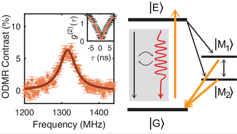
abstract = {Hexagonal boron nitride (h-BN) hosts pure single-photon emitters that have shown evidence of optically detected electronic spin dynamics. However, the electrical and chemical structures of these optically addressable spins are unknown, and the nature of their spin-optical interactions remains mysterious. Here, we use time-domain optical and microwave experiments to characterize a single emitter in h-BN exhibiting room temperature optically detected magnetic resonance. Using dynamical simulations, we constrain and quantify transition rates in the model, and we design optical control protocols that optimize the signal-to-noise ratio for spin readout. This constitutes a necessary step toward quantum control of spin states in h-BN.},
keywords = {2-dimensional systems, First-principles calculations, photon emission correlation spectroscopy, photon statistics, point defects},
pubstate = {published},
tppubtype = {article}
}
Keneipp, Rachael N.; Gusdorff, Jordan A.; Bhatia, Pia; Shin, Trey T.; Bassett, Lee C.; Drndić, Marija
Nanoscale Sculpting of Hexagonal Boron Nitride with an Electron Beam Journal Article
In: Journal of Physical Chemistry C, vol. 128, no. 21, pp. 8741–8749, 2024.
Abstract | Links | BibTeX | Tags: 2-dimensional systems, color centers, photoluminescence, point defects
@article{Keneipp2024,
title = {Nanoscale Sculpting of Hexagonal Boron Nitride with an Electron Beam},
author = {Rachael N. Keneipp and Jordan A. Gusdorff and Pia Bhatia and Trey T. Shin and Lee C. Bassett and Marija Drndić},
url = {https://pubs.acs.org/doi/full/10.1021/acs.jpcc.4c02038},
doi = {10.1021/acs.jpcc.4c02038},
year = {2024},
date = {2024-05-17},
journal = {Journal of Physical Chemistry C},
volume = {128},
number = {21},
pages = {8741–8749},
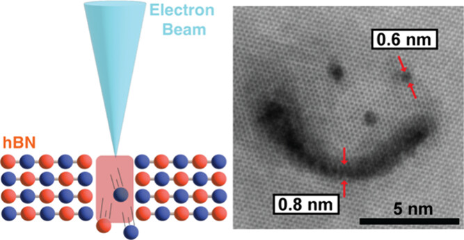
abstract = {Creating sub- to few-nanometer defects and nanopores in hexagonal boron nitride (hBN) opens opportunities for engineering quantum emitters and for nanofluidic and sensing applications. Using the electron beam in the aberration-corrected scanning transmission electron microscope, we demonstrate modification, thinning, and drilling of features in few-layer hBN membranes (∼5 to 20 nm-thick). The atomic composition is monitored with electron energy loss spectroscopy, which also facilitates drift correction. We report effects of electron beam energy and exposure times on defect size and structure. While previous studies focused on beam energies of ≤80 keV to avoid material damage, we show that drilling is favorable at a higher beam energy of 200 keV. The drilling rate at 200 keV is about 10 times larger than at 80 keV (∼1.2 vs 0.1 nm/min), and smaller pores are achievable with minimized damage to the surrounding material. Thinned hBN nanoscale features demonstrate enhanced emission via photoluminescence spectroscopy.},
keywords = {2-dimensional systems, color centers, photoluminescence, point defects},
pubstate = {published},
tppubtype = {article}
}
Fishman, Rebecca E. K.; Patel, Raj N.; Hopper, David A.; Huang, Tzu-Yung; Bassett, Lee C.
Photon emission correlation spectroscopy as an analytical tool for quantum defects Journal Article
In: PRX Quantum, vol. 4, pp. 010202, 2023.
Abstract | Links | BibTeX | Tags: First-principles calculations, Materials Physics, Optics, photon emission correlation spectroscopy, photon statistics, point defects, quantum defects
@article{Fishman2021,
title = {Photon emission correlation spectroscopy as an analytical tool for quantum defects},
author = {Rebecca E. K. Fishman and Raj N. Patel and David A. Hopper and Tzu-Yung Huang and Lee C. Bassett},
url = {https://journals.aps.org/prxquantum/abstract/10.1103/PRXQuantum.4.010202
https://arxiv.org/abs/2111.01252},
doi = {10.1103/PRXQuantum.4.010202},
year = {2023},
date = {2023-03-06},
journal = {PRX Quantum},
volume = {4},
pages = {010202},
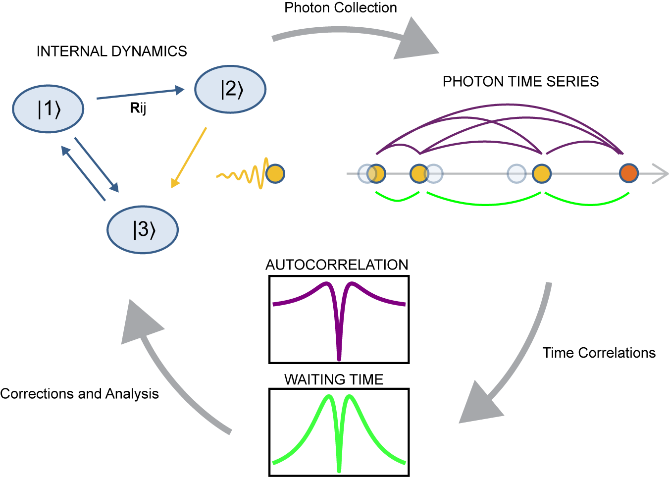
abstract = {Photon emission correlation spectroscopy has a long history in the study of atoms, molecules, and, more recently, solid-state quantum defects. In solid-state systems, its most common use is as an indicator of single-photon emission, a key property for quantum technology. However, photon correlation data can provide a wealth of information about quantum emitters beyond their single-photon purity−information that can reveal details about an emitter's electronic structure and optical dynamics that are hidden by other spectroscopy techniques. We present a standardized framework for using photon emission correlation spectroscopy to study quantum emitters, including discussion of theory, data acquisition, analysis, and interpretation. We highlight nuances and best practices regarding the commonly used g(2)(τ=0)<0.5 test for single-photon emission. Finally, we illustrate how this experimental technique can be paired with optical dynamics simulations to formulate an electronic model for unknown quantum emitters, enabling the design of quantum control protocols and assessment of their suitability for quantum information science applications.},
keywords = {First-principles calculations, Materials Physics, Optics, photon emission correlation spectroscopy, photon statistics, point defects, quantum defects},
pubstate = {published},
tppubtype = {article}
}

Patel, Raj N.; Hopper, David A.; Gusdorff, Jordan A.; Turiansky, Mark E.; Huang, Tzu-Yung; Fishman, Rebecca E. K.; Porat, Benjamin; de Walle, Chris G. Van; Bassett, Lee C.
Probing the Optical Dynamics of Quantum Emitters in Hexagonal Boron Nitride Journal Article
In: PRX Quantum, vol. 3, no. 3, pp. 030331, 2022.
Abstract | Links | BibTeX | Tags: 2-dimensional systems, color centers, photon emission correlation spectroscopy, photon statistics, point defects, quantum optics, single-photon sources
@article{Patel2022,

title = {Probing the Optical Dynamics of Quantum Emitters in Hexagonal Boron Nitride},

author = {Raj N. Patel and David A. Hopper and Jordan A. Gusdorff and Mark E. Turiansky and Tzu-Yung Huang and Rebecca E. K. Fishman and Benjamin Porat and Chris G. Van de Walle and Lee C. Bassett},

url = {https://journals.aps.org/prxquantum/abstract/10.1103/PRXQuantum.3.030331},

doi = {10.1103/PRXQuantum.3.030331},

year  = {2022},

date = {2022-09-01},

journal = {PRX Quantum},

volume = {3},

number = {3},

pages = {030331},

abstract = {Hexagonal boron nitride is a van der Waals material that hosts visible-wavelength quantum emitters at room temperature. However, experimental identification of the quantum emitters’ electronic structure is lacking, and key details of their charge and spin properties remain unknown. Here, we probe the optical dynamics of quantum emitters in hexagonal boron nitride using photon emission correlation spectroscopy. Several quantum emitters exhibit ideal single-photon emission with noise-limited photon antibunching, g(2)(0)=0. The photoluminescence emission lineshapes are consistent with individual vibronic transitions. However, polarization-resolved excitation and emission suggests the role of multiple optical transitions, and photon emission correlation spectroscopy reveals complicated optical dynamics associated with excitation and relaxation through multiple electronic excited states. We compare the experimental results to quantitative optical dynamics simulations, develop electronic structure models that are consistent with the observations, and discuss the results in the context of ab initio theoretical calculations.},

keywords = {2-dimensional systems, color centers, photon emission correlation spectroscopy, photon statistics, point defects, quantum optics, single-photon sources},

pubstate = {published},

tppubtype = {article}

}
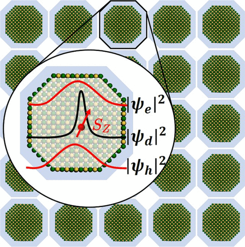
Kagan, Cherie R.; Bassett, Lee C.; Murray, Christopher B.; Thompson, Sarah M.
Colloidal Quantum Dots as Platforms for Quantum Information Science Journal Article
In: Chemical Reviews, 2020.
Abstract | Links | BibTeX | Tags: point defects, quantum dots, quantum information science
@article{Kagan2020,

title = {Colloidal Quantum Dots as Platforms for Quantum Information Science},

author = {Cherie R. Kagan and Lee C. Bassett and Christopher B. Murray and Sarah M. Thompson},

url = {https://pubs.acs.org/doi/10.1021/acs.chemrev.0c00831},

doi = {10.1021/acs.chemrev.0c00831},

year  = {2020},

date = {2020-12-29},

journal = {Chemical Reviews},

abstract = {Colloidal quantum dots (QDs) are nanoscale semiconductor crystals with surface ligands that enable their dispersion in solvents. Quantum confinement effects facilitate wave function engineering to sculpt the spatial distribution of charge and spin states and thus the energy and dynamics of QD optical transitions. Colloidal QDs can be integrated in devices using solution-based assembly methods to position single QDs and to create ordered QD arrays. Here, we describe the synthesis, assembly, and photophysical properties of colloidal QDs that have captured scientific imagination and have been harnessed in optical applications. We focus especially on the current understanding of their quantum coherent effects and opportunities to exploit QDs as platforms for quantum information science. Freedom in QD design to isolate and control the quantum mechanical properties of charge, spin, and light presents various approaches to create systems with robust, addressable quantum states. We consider the attributes of QDs for optically addressable qubits in emerging quantum computation, sensing, simulation, and communication technologies, e.g., as robust sources of indistinguishable, single photons that can be integrated into photonic structures to amplify, direct, and tune their emission or as hosts for isolated, coherent spin states that can be coupled to light or to other spins in QD arrays.},

keywords = {point defects, quantum dots, quantum information science},

pubstate = {published},

tppubtype = {article}

}
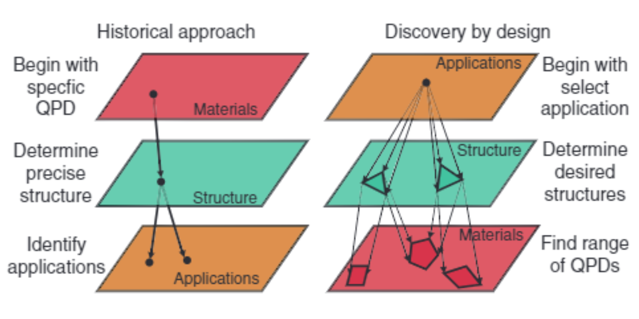
Bassett, L. C.; Alkauskas, A.; Exarhos, A. L.; Fu, K. -M. C.
Quantum defects by design Journal Article
In: Nanophotonics, vol. 8, no. 11, 2019.
Abstract | Links | BibTeX | Tags: Nanophotonics, optical sources, point defects, Quantum Control
@article{Bassett2019b,

title = {Quantum defects by design},

author = {L. C. Bassett and A. Alkauskas and A. L. Exarhos and K.-M. C. Fu},

url = {https://www.degruyter.com/view/journals/nanoph/8/11/article-p1867.xml},

year  = {2019},

date = {2019-10-04},

journal = {Nanophotonics},

volume = {8},

number = {11},

abstract = {Part of Special Issue on Quantum Nanophotonics in Emerging Materials.


Miniaturization of electronic and opto-electronic semiconductor devices has been happening ever since the first such devices appeared. Eventually, one can envision a device that is composed of just a few atoms. As these atoms ideally should not float in free space, but should be embedded in a solid-state matrix, this naturally brings one to the concept of a point defect (an impurity atom or complex of atoms) as the ultimate electronic or opto-electronic device. At such tiny length scales the behavior of physical systems is governed by the laws of quantum mechanics. Therefore, it is no surprise that an increasing number of point defects are being considered as building blocks for various applications in the field of quantum information science; more specifically, in quantum sensing, quantum communication, and quantum computing [1], [2], [3], [4]. We refer to these desirable defects as quantum point defects (QPDs). Prominent examples include the nitrogen-vacancy (NV) center in diamond, the silicon-vacancy (SiV) center in diamond, the divacancy in silicon carbide, and rare-earth impurities in complex oxides.},

keywords = {Nanophotonics, optical sources, point defects, Quantum Control},

pubstate = {published},

tppubtype = {article}

}
Miniaturization of electronic and opto-electronic semiconductor devices has been happening ever since the first such devices appeared. Eventually, one can envision a device that is composed of just a few atoms. As these atoms ideally should not float in free space, but should be embedded in a solid-state matrix, this naturally brings one to the concept of a point defect (an impurity atom or complex of atoms) as the ultimate electronic or opto-electronic device. At such tiny length scales the behavior of physical systems is governed by the laws of quantum mechanics. Therefore, it is no surprise that an increasing number of point defects are being considered as building blocks for various applications in the field of quantum information science; more specifically, in quantum sensing, quantum communication, and quantum computing [1], [2], [3], [4]. We refer to these desirable defects as quantum point defects (QPDs). Prominent examples include the nitrogen-vacancy (NV) center in diamond, the silicon-vacancy (SiV) center in diamond, the divacancy in silicon carbide, and rare-earth impurities in complex oxides.
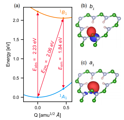
Turiansky, M E; Alkauskas, A; Bassett, L C; de Walle, Van C G
Dangling bonds in hexagonal boron nitride as single-photon emitters Journal Article
In: Physical Review Letters, vol. 123, no. 12, pp. 127401, 2019, ISSN: 1079-7114.
Abstract | Links | BibTeX | Tags: 2-dimensional systems, Condensed Matter, First-principles calculations, Optical absorption spectroscopy, Optical microcavities, optical sources, point defects, Quantum wells, Semiconductor compounds
@article{Turiansky2019,

title = {Dangling bonds in hexagonal boron nitride as single-photon emitters},

author = {M E Turiansky and A Alkauskas and L C Bassett and Van C G de Walle},

url = {https://journals.aps.org/prl/abstract/10.1103/PhysRevLett.123.127401},

doi = {10.1103},

issn = {1079-7114},

year  = {2019},

date = {2019-09-16},

journal = {Physical Review Letters},

volume = {123},

number = {12},

pages = {127401},

abstract = {Hexagonal boron nitride has been found to host color centers that exhibit single-photon emission, but the microscopic origin of these emitters is unknown. We propose boron dangling bonds as the likely source of the observed single-photon emission around 2 eV. An optical transition where an electron is excited from a doubly occupied boron dangling bond to a localized B pz state gives rise to a zero-phonon line of 2.06 eV and emission with a Huang-Rhys factor of 2.3. This transition is linearly polarized with the absorptive and emissive dipole aligned. Because of the energetic position of the states within the band gap, indirect excitation through the conduction band will occur for sufficiently large excitation energies, leading to the misalignment of the absorptive and emissive dipoles seen in experiment. Our calculations predict a singlet ground state and the existence of a metastable triplet state, in agreement with experiment.},

keywords = {2-dimensional systems, Condensed Matter, First-principles calculations, Optical absorption spectroscopy, Optical microcavities, optical sources, point defects, Quantum wells, Semiconductor compounds},

pubstate = {published},

tppubtype = {article}

}
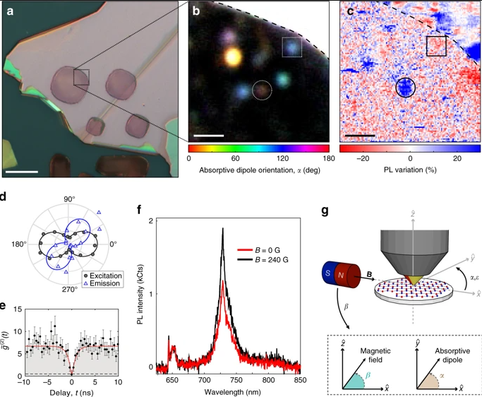
Exarhos, A L; Hopper, D A; Patel, R N; Doherty, M W; Bassett, L C
Magnetic-field-dependent quantum emission in hexagonal boron nitride at room temperature Journal Article
In: Nature Communications, vol. 10, no. 222, 2019.
Abstract | Links | BibTeX | Tags: 2-dimensional systems, point defects
@article{Exarhos2019,
title = {Magnetic-field-dependent quantum emission in hexagonal boron nitride at room temperature},
author = {A L Exarhos and D A Hopper and R N Patel and M W Doherty and L C Bassett},
url = {https://www.nature.com/articles/s41467-018-08185-8
https://www.nature.com/collections/rcdhyvxytb
https://spectrum.ieee.org/tech-talk/semiconductors/nanotechnology/qubits-and-nanosensors-in-a-2d-material
https://medium.com/penn-engineering/penn-engineers-develop-room-temperature-two-dimensional-platform-for-quantum-technology-cae3a5c0d8f9},
year = {2019},
date = {2019-01-15},
journal = {Nature Communications},
volume = {10},
number = {222},
abstract = {Selected as Editor's Highlight (linked)
Press coverage in IEEE Spectrum and Penn Medium (linked)
Optically addressable spins associated with defects in wide-bandgap semiconductors are versatile platforms for quantum information processing and nanoscale sensing, where spin-dependent inter-system crossing transitions facilitate optical spin initialization and readout. Recently, the van der Waals material hexagonal boron nitride (h-BN) has emerged as a robust host for quantum emitters, promising efficient photon extraction and atom-scale engineering, but observations of spin-related effects have remained thus far elusive. Here, we report room-temperature observations of strongly anisotropic photoluminescence patterns as a function of applied magnetic field for select quantum emitters in h-BN. Field-dependent variations in the steady-state photoluminescence and photon emission statistics are consistent with an electronic model featuring a spin-dependent inter-system crossing between triplet and singlet manifolds, indicating that optically-addressable spin defects are present in h-BN.},
keywords = {2-dimensional systems, point defects},
pubstate = {published},
tppubtype = {article}
}
Press coverage in IEEE Spectrum and Penn Medium (linked)
Optically addressable spins associated with defects in wide-bandgap semiconductors are versatile platforms for quantum information processing and nanoscale sensing, where spin-dependent inter-system crossing transitions facilitate optical spin initialization and readout. Recently, the van der Waals material hexagonal boron nitride (h-BN) has emerged as a robust host for quantum emitters, promising efficient photon extraction and atom-scale engineering, but observations of spin-related effects have remained thus far elusive. Here, we report room-temperature observations of strongly anisotropic photoluminescence patterns as a function of applied magnetic field for select quantum emitters in h-BN. Field-dependent variations in the steady-state photoluminescence and photon emission statistics are consistent with an electronic model featuring a spin-dependent inter-system crossing between triplet and singlet manifolds, indicating that optically-addressable spin defects are present in h-BN.
Exarhos, A L; Hopper, D A; Grote, R R; Alkauskas, A; Bassett, L C
Optical signatures of quantum emitters in suspended hexagonal boron nitride Journal Article
In: ACS Nano, vol. 11, pp. 3328-3336, 2017.
Abstract | Links | BibTeX | Tags: 2-dimensional systems, Condensed Matter, optical sources, point defects
@article{Exarhos2017,

title = {Optical signatures of quantum emitters in suspended hexagonal boron nitride},

author = {A L Exarhos and D A Hopper and R R Grote and A Alkauskas and L C Bassett},

url = {https://pubs.acs.org/doi/abs/10.1021/acsnano.7b00665},

year  = {2017},

date = {2017-03-07},

journal = {ACS Nano},

volume = {11},

pages = {3328-3336},

abstract = {Hexagonal boron nitride (h-BN) is rapidly emerging as an attractive material for solid-state quantum engineering. Analogously to three-dimensional wide-band-gap semiconductors such as diamond, h-BN hosts isolated defects exhibiting visible fluorescence at room temperature, and the ability to position such quantum emitters within a two-dimensional material promises breakthrough advances in quantum sensing, photonics, and other quantum technologies. Critical to such applications is an understanding of the physics underlying h-BN’s quantum emission. We report the creation and characterization of visible single-photon sources in suspended, single-crystal, h-BN films. With substrate interactions eliminated, we study the spectral, temporal, and spatial characteristics of the defects’ optical emission. Theoretical analysis of the defects’ spectra reveals similarities in vibronic coupling to h-BN phonon modes despite widely varying fluorescence wavelengths, and a statistical analysis of the polarized emission from many emitters throughout the same single-crystal flake uncovers a weak correlation between the optical dipole orientations of some defects and h-BN’s primitive crystallographic axes, despite a clear misalignment for other dipoles. These measurements constrain possible defect models and, moreover, suggest that several classes of emitters can exist simultaneously throughout free-standing h-BN, whether they be different defects, different charge states of the same defect, or the result of strong local perturbations.},

keywords = {2-dimensional systems, Condensed Matter, optical sources, point defects},

pubstate = {published},

tppubtype = {article}

}
Bassett, L C; Heremans, F J; Christle, D J; Yale, C G; Burkard, G; Buckley, B B; Awschalom, D D
Ultrafast optical control of orbital and spin dynamics in a solid-state defect Journal Article
In: Science, vol. 345, pp. 1333-1337, 2014.
Abstract | Links | BibTeX | Tags: Condensed Matter, point defects, spin readout
@article{Bassett2014,

title = {Ultrafast optical control of orbital and spin dynamics in a solid-state defect},

author = {L C Bassett and F J Heremans and D J Christle and C G Yale and G Burkard and B B Buckley and D D Awschalom},

url = {https://science.sciencemag.org/content/345/6202/1333},

year  = {2014},

date = {2014-09-12},

journal = {Science},

volume = {345},

pages = {1333-1337},

abstract = {Atom-scale defects in semiconductors are promising building blocks for quantum devices, but our understanding of their material-dependent electronic structure, optical interactions, and dissipation mechanisms is lacking. Using picosecond resonant pulses of light, we study the coherent orbital and spin dynamics of a single nitrogen-vacancy center in diamond over time scales spanning six orders of magnitude. We develop a time-domain quantum tomography technique to precisely map the defect’s excited-state Hamiltonian and exploit the excited-state dynamics to control its ground-state spin with optical pulses alone. These techniques generalize to other optically addressable nanoscale spin systems and serve as powerful tools to characterize and control spin qubits for future applications in quantum technology.},

keywords = {Condensed Matter, point defects, spin readout},

pubstate = {published},

tppubtype = {article}

}
2024
Breitweiser, S. Alex; Ouellet, Mathieu; Huang, Tzu-Yung; Taminiau, Tim H.; Bassett, Lee C.
Quadrupolar resonance spectroscopy of individual nuclei using a room-temperature quantum sensor Journal Article
In: Nano Letters, vol. 24, iss. 51, pp. 16253-16260, 2024.
@article{Breitweiser2024,

title = {Quadrupolar resonance spectroscopy of individual nuclei using a room-temperature quantum sensor},

author = {S. Alex Breitweiser and Mathieu Ouellet and Tzu-Yung Huang and Tim H. Taminiau and Lee C. Bassett},

url = {https://pubs.acs.org/doi/abs/10.1021/acs.nanolett.4c04112

https://arxiv.org/abs/2405.14859},

year  = {2024},

date = {2024-12-12},

urldate = {2024-12-12},

journal = {Nano Letters},

volume = {24},

issue = {51},

pages = {16253-16260},

abstract = {Nuclear quadrupolar resonance (NQR) spectroscopy reveals chemical bonding patterns in materials and molecules through the unique coupling between nuclear spins and local fields. However, traditional NQR techniques require macroscopic ensembles of nuclei to yield a detectable signal, which obscures molecule-to-molecule variations. Solid-state spin qubits, such as the nitrogen-vacancy (NV) center in diamond, facilitate the detection and control of individual nuclei through their local magnetic couplings. Here, we use NV centers to perform NQR spectroscopy on their associated nitrogen-14 (14N) nuclei at room temperature. In mapping the nuclear quadrupolar Hamiltonian, we resolve minute variations between individual nuclei. The measurements reveal correlations between the Hamiltonian parameters associated with the NV center’s electronic and nuclear spin states, as well as a previously unreported symmetry-breaking quadrupolar term. We further design pulse sequences to initialize, read out, and control the quantum evolution of the 14N nuclear state using the nuclear quadrupolar Hamiltonian.},

keywords = {},

pubstate = {published},

tppubtype = {article}

}
Patel, Raj N.; Fishman, Rebecca E. K.; Huang, Tzu-Yung; Gusdorff, Jordan A.; Fehr, David A.; Hopper, David A.; Breitweiser, S. Alex; Porat, Benjamin; Flatté, Michael E.; Bassett, Lee C.
Room Temperature Dynamics of an Optically Addressable Single Spin in Hexagonal Boron Nitride Journal Article
In: Nano Letters, vol. 24, iss. 25, pp. 7623-7628, 2024.
@article{Patel2024,

title = {Room Temperature Dynamics of an Optically Addressable Single Spin in Hexagonal Boron Nitride},

author = {Raj N. Patel and Rebecca E. K. Fishman and Tzu-Yung Huang and Jordan A. Gusdorff and David A. Fehr and David A. Hopper and S. Alex Breitweiser and Benjamin Porat and Michael E. Flatté and Lee C. Bassett},

url = {https://pubs.acs.org/doi/abs/10.1021/acs.nanolett.4c01333

https://arxiv.org/abs/2309.05604},

doi = {10.1021/acs.nanolett.4c01333},

year  = {2024},

date = {2024-06-11},

urldate = {2024-06-11},

journal = {Nano Letters},

volume = {24},

issue = {25},

pages = {7623-7628},

abstract = {Hexagonal boron nitride (h-BN) hosts pure single-photon emitters that have shown evidence of optically detected electronic spin dynamics. However, the electrical and chemical structures of these optically addressable spins are unknown, and the nature of their spin-optical interactions remains mysterious. Here, we use time-domain optical and microwave experiments to characterize a single emitter in h-BN exhibiting room temperature optically detected magnetic resonance. Using dynamical simulations, we constrain and quantify transition rates in the model, and we design optical control protocols that optimize the signal-to-noise ratio for spin readout. This constitutes a necessary step toward quantum control of spin states in h-BN.},

keywords = {},

pubstate = {published},

tppubtype = {article}

}
Keneipp, Rachael N.; Gusdorff, Jordan A.; Bhatia, Pia; Shin, Trey T.; Bassett, Lee C.; Drndić, Marija
Nanoscale Sculpting of Hexagonal Boron Nitride with an Electron Beam Journal Article
In: Journal of Physical Chemistry C, vol. 128, no. 21, pp. 8741–8749, 2024.
@article{Keneipp2024,

title = {Nanoscale Sculpting of Hexagonal Boron Nitride with an Electron Beam},

author = {Rachael N. Keneipp and Jordan A. Gusdorff and Pia Bhatia and Trey T. Shin and Lee C. Bassett and Marija Drndić},

url = {https://pubs.acs.org/doi/full/10.1021/acs.jpcc.4c02038},

doi = {10.1021/acs.jpcc.4c02038},

year  = {2024},

date = {2024-05-17},

journal = {Journal of Physical Chemistry C},

volume = {128},

number = {21},

pages = {8741–8749},

abstract = {Creating sub- to few-nanometer defects and nanopores in hexagonal boron nitride (hBN) opens opportunities for engineering quantum emitters and for nanofluidic and sensing applications. Using the electron beam in the aberration-corrected scanning transmission electron microscope, we demonstrate modification, thinning, and drilling of features in few-layer hBN membranes (∼5 to 20 nm-thick). The atomic composition is monitored with electron energy loss spectroscopy, which also facilitates drift correction. We report effects of electron beam energy and exposure times on defect size and structure. While previous studies focused on beam energies of ≤80 keV to avoid material damage, we show that drilling is favorable at a higher beam energy of 200 keV. The drilling rate at 200 keV is about 10 times larger than at 80 keV (∼1.2 vs 0.1 nm/min), and smaller pores are achievable with minimized damage to the surrounding material. Thinned hBN nanoscale features demonstrate enhanced emission via photoluminescence spectroscopy.},

keywords = {},

pubstate = {published},

tppubtype = {article}

}
2023
Fishman, Rebecca E. K.; Patel, Raj N.; Hopper, David A.; Huang, Tzu-Yung; Bassett, Lee C.
Photon emission correlation spectroscopy as an analytical tool for quantum defects Journal Article
In: PRX Quantum, vol. 4, pp. 010202, 2023.
@article{Fishman2021,

title = {Photon emission correlation spectroscopy as an analytical tool for quantum defects},

author = {Rebecca E. K. Fishman and Raj N. Patel and David A. Hopper and Tzu-Yung Huang and Lee C. Bassett},

url = {https://journals.aps.org/prxquantum/abstract/10.1103/PRXQuantum.4.010202

https://arxiv.org/abs/2111.01252},

doi = {10.1103/PRXQuantum.4.010202},

year  = {2023},

date = {2023-03-06},

journal = {PRX Quantum},

volume = {4},

pages = {010202},

abstract = {Photon emission correlation spectroscopy has a long history in the study of atoms, molecules, and, more recently, solid-state quantum defects. In solid-state systems, its most common use is as an indicator of single-photon emission, a key property for quantum technology. However, photon correlation data can provide a wealth of information about quantum emitters beyond their single-photon purity−information that can reveal details about an emitter's electronic structure and optical dynamics that are hidden by other spectroscopy techniques. We present a standardized framework for using photon emission correlation spectroscopy to study quantum emitters, including discussion of theory, data acquisition, analysis, and interpretation. We highlight nuances and best practices regarding the commonly used g(2)(τ=0)<0.5 test for single-photon emission. Finally, we illustrate how this experimental technique can be paired with optical dynamics simulations to formulate an electronic model for unknown quantum emitters, enabling the design of quantum control protocols and assessment of their suitability for quantum information science applications.},

keywords = {},

pubstate = {published},

tppubtype = {article}

}
2022
Patel, Raj N.; Hopper, David A.; Gusdorff, Jordan A.; Turiansky, Mark E.; Huang, Tzu-Yung; Fishman, Rebecca E. K.; Porat, Benjamin; de Walle, Chris G. Van; Bassett, Lee C.
Probing the Optical Dynamics of Quantum Emitters in Hexagonal Boron Nitride Journal Article
In: PRX Quantum, vol. 3, no. 3, pp. 030331, 2022.
@article{Patel2022,

title = {Probing the Optical Dynamics of Quantum Emitters in Hexagonal Boron Nitride},

author = {Raj N. Patel and David A. Hopper and Jordan A. Gusdorff and Mark E. Turiansky and Tzu-Yung Huang and Rebecca E. K. Fishman and Benjamin Porat and Chris G. Van de Walle and Lee C. Bassett},

url = {https://journals.aps.org/prxquantum/abstract/10.1103/PRXQuantum.3.030331},

doi = {10.1103/PRXQuantum.3.030331},

year  = {2022},

date = {2022-09-01},

journal = {PRX Quantum},

volume = {3},

number = {3},

pages = {030331},

abstract = {Hexagonal boron nitride is a van der Waals material that hosts visible-wavelength quantum emitters at room temperature. However, experimental identification of the quantum emitters’ electronic structure is lacking, and key details of their charge and spin properties remain unknown. Here, we probe the optical dynamics of quantum emitters in hexagonal boron nitride using photon emission correlation spectroscopy. Several quantum emitters exhibit ideal single-photon emission with noise-limited photon antibunching, g(2)(0)=0. The photoluminescence emission lineshapes are consistent with individual vibronic transitions. However, polarization-resolved excitation and emission suggests the role of multiple optical transitions, and photon emission correlation spectroscopy reveals complicated optical dynamics associated with excitation and relaxation through multiple electronic excited states. We compare the experimental results to quantitative optical dynamics simulations, develop electronic structure models that are consistent with the observations, and discuss the results in the context of ab initio theoretical calculations.},

keywords = {},

pubstate = {published},

tppubtype = {article}

}
2020
Kagan, Cherie R.; Bassett, Lee C.; Murray, Christopher B.; Thompson, Sarah M.
Colloidal Quantum Dots as Platforms for Quantum Information Science Journal Article
In: Chemical Reviews, 2020.
@article{Kagan2020,

title = {Colloidal Quantum Dots as Platforms for Quantum Information Science},

author = {Cherie R. Kagan and Lee C. Bassett and Christopher B. Murray and Sarah M. Thompson},

url = {https://pubs.acs.org/doi/10.1021/acs.chemrev.0c00831},

doi = {10.1021/acs.chemrev.0c00831},

year  = {2020},

date = {2020-12-29},

journal = {Chemical Reviews},

abstract = {Colloidal quantum dots (QDs) are nanoscale semiconductor crystals with surface ligands that enable their dispersion in solvents. Quantum confinement effects facilitate wave function engineering to sculpt the spatial distribution of charge and spin states and thus the energy and dynamics of QD optical transitions. Colloidal QDs can be integrated in devices using solution-based assembly methods to position single QDs and to create ordered QD arrays. Here, we describe the synthesis, assembly, and photophysical properties of colloidal QDs that have captured scientific imagination and have been harnessed in optical applications. We focus especially on the current understanding of their quantum coherent effects and opportunities to exploit QDs as platforms for quantum information science. Freedom in QD design to isolate and control the quantum mechanical properties of charge, spin, and light presents various approaches to create systems with robust, addressable quantum states. We consider the attributes of QDs for optically addressable qubits in emerging quantum computation, sensing, simulation, and communication technologies, e.g., as robust sources of indistinguishable, single photons that can be integrated into photonic structures to amplify, direct, and tune their emission or as hosts for isolated, coherent spin states that can be coupled to light or to other spins in QD arrays.},

keywords = {},

pubstate = {published},

tppubtype = {article}

}
2019
Bassett, L. C.; Alkauskas, A.; Exarhos, A. L.; Fu, K. -M. C.
Quantum defects by design Journal Article
In: Nanophotonics, vol. 8, no. 11, 2019.
@article{Bassett2019b,

title = {Quantum defects by design},

author = {L. C. Bassett and A. Alkauskas and A. L. Exarhos and K.-M. C. Fu},

url = {https://www.degruyter.com/view/journals/nanoph/8/11/article-p1867.xml},

year  = {2019},

date = {2019-10-04},

journal = {Nanophotonics},

volume = {8},

number = {11},

abstract = {Part of Special Issue on Quantum Nanophotonics in Emerging Materials.


Miniaturization of electronic and opto-electronic semiconductor devices has been happening ever since the first such devices appeared. Eventually, one can envision a device that is composed of just a few atoms. As these atoms ideally should not float in free space, but should be embedded in a solid-state matrix, this naturally brings one to the concept of a point defect (an impurity atom or complex of atoms) as the ultimate electronic or opto-electronic device. At such tiny length scales the behavior of physical systems is governed by the laws of quantum mechanics. Therefore, it is no surprise that an increasing number of point defects are being considered as building blocks for various applications in the field of quantum information science; more specifically, in quantum sensing, quantum communication, and quantum computing [1], [2], [3], [4]. We refer to these desirable defects as quantum point defects (QPDs). Prominent examples include the nitrogen-vacancy (NV) center in diamond, the silicon-vacancy (SiV) center in diamond, the divacancy in silicon carbide, and rare-earth impurities in complex oxides.},

keywords = {},

pubstate = {published},

tppubtype = {article}

}
Miniaturization of electronic and opto-electronic semiconductor devices has been happening ever since the first such devices appeared. Eventually, one can envision a device that is composed of just a few atoms. As these atoms ideally should not float in free space, but should be embedded in a solid-state matrix, this naturally brings one to the concept of a point defect (an impurity atom or complex of atoms) as the ultimate electronic or opto-electronic device. At such tiny length scales the behavior of physical systems is governed by the laws of quantum mechanics. Therefore, it is no surprise that an increasing number of point defects are being considered as building blocks for various applications in the field of quantum information science; more specifically, in quantum sensing, quantum communication, and quantum computing [1], [2], [3], [4]. We refer to these desirable defects as quantum point defects (QPDs). Prominent examples include the nitrogen-vacancy (NV) center in diamond, the silicon-vacancy (SiV) center in diamond, the divacancy in silicon carbide, and rare-earth impurities in complex oxides.
Turiansky, M E; Alkauskas, A; Bassett, L C; de Walle, Van C G
Dangling bonds in hexagonal boron nitride as single-photon emitters Journal Article
In: Physical Review Letters, vol. 123, no. 12, pp. 127401, 2019, ISSN: 1079-7114.
@article{Turiansky2019,

title = {Dangling bonds in hexagonal boron nitride as single-photon emitters},

author = {M E Turiansky and A Alkauskas and L C Bassett and Van C G de Walle},

url = {https://journals.aps.org/prl/abstract/10.1103/PhysRevLett.123.127401},

doi = {10.1103},

issn = {1079-7114},

year  = {2019},

date = {2019-09-16},

journal = {Physical Review Letters},

volume = {123},

number = {12},

pages = {127401},

abstract = {Hexagonal boron nitride has been found to host color centers that exhibit single-photon emission, but the microscopic origin of these emitters is unknown. We propose boron dangling bonds as the likely source of the observed single-photon emission around 2 eV. An optical transition where an electron is excited from a doubly occupied boron dangling bond to a localized B pz state gives rise to a zero-phonon line of 2.06 eV and emission with a Huang-Rhys factor of 2.3. This transition is linearly polarized with the absorptive and emissive dipole aligned. Because of the energetic position of the states within the band gap, indirect excitation through the conduction band will occur for sufficiently large excitation energies, leading to the misalignment of the absorptive and emissive dipoles seen in experiment. Our calculations predict a singlet ground state and the existence of a metastable triplet state, in agreement with experiment.},

keywords = {},

pubstate = {published},

tppubtype = {article}

}
Exarhos, A L; Hopper, D A; Patel, R N; Doherty, M W; Bassett, L C
Magnetic-field-dependent quantum emission in hexagonal boron nitride at room temperature Journal Article
In: Nature Communications, vol. 10, no. 222, 2019.
@article{Exarhos2019,
title = {Magnetic-field-dependent quantum emission in hexagonal boron nitride at room temperature},
author = {A L Exarhos and D A Hopper and R N Patel and M W Doherty and L C Bassett},
url = {https://www.nature.com/articles/s41467-018-08185-8
https://www.nature.com/collections/rcdhyvxytb
https://spectrum.ieee.org/tech-talk/semiconductors/nanotechnology/qubits-and-nanosensors-in-a-2d-material
https://medium.com/penn-engineering/penn-engineers-develop-room-temperature-two-dimensional-platform-for-quantum-technology-cae3a5c0d8f9},
year = {2019},
date = {2019-01-15},
journal = {Nature Communications},
volume = {10},
number = {222},
abstract = {Selected as Editor's Highlight (linked)
Press coverage in IEEE Spectrum and Penn Medium (linked)
Optically addressable spins associated with defects in wide-bandgap semiconductors are versatile platforms for quantum information processing and nanoscale sensing, where spin-dependent inter-system crossing transitions facilitate optical spin initialization and readout. Recently, the van der Waals material hexagonal boron nitride (h-BN) has emerged as a robust host for quantum emitters, promising efficient photon extraction and atom-scale engineering, but observations of spin-related effects have remained thus far elusive. Here, we report room-temperature observations of strongly anisotropic photoluminescence patterns as a function of applied magnetic field for select quantum emitters in h-BN. Field-dependent variations in the steady-state photoluminescence and photon emission statistics are consistent with an electronic model featuring a spin-dependent inter-system crossing between triplet and singlet manifolds, indicating that optically-addressable spin defects are present in h-BN.},
keywords = {},
pubstate = {published},
tppubtype = {article}
}
Press coverage in IEEE Spectrum and Penn Medium (linked)
Optically addressable spins associated with defects in wide-bandgap semiconductors are versatile platforms for quantum information processing and nanoscale sensing, where spin-dependent inter-system crossing transitions facilitate optical spin initialization and readout. Recently, the van der Waals material hexagonal boron nitride (h-BN) has emerged as a robust host for quantum emitters, promising efficient photon extraction and atom-scale engineering, but observations of spin-related effects have remained thus far elusive. Here, we report room-temperature observations of strongly anisotropic photoluminescence patterns as a function of applied magnetic field for select quantum emitters in h-BN. Field-dependent variations in the steady-state photoluminescence and photon emission statistics are consistent with an electronic model featuring a spin-dependent inter-system crossing between triplet and singlet manifolds, indicating that optically-addressable spin defects are present in h-BN.
2017
Exarhos, A L; Hopper, D A; Grote, R R; Alkauskas, A; Bassett, L C
Optical signatures of quantum emitters in suspended hexagonal boron nitride Journal Article
In: ACS Nano, vol. 11, pp. 3328-3336, 2017.
@article{Exarhos2017,

title = {Optical signatures of quantum emitters in suspended hexagonal boron nitride},

author = {A L Exarhos and D A Hopper and R R Grote and A Alkauskas and L C Bassett},

url = {https://pubs.acs.org/doi/abs/10.1021/acsnano.7b00665},

year  = {2017},

date = {2017-03-07},

journal = {ACS Nano},

volume = {11},

pages = {3328-3336},

abstract = {Hexagonal boron nitride (h-BN) is rapidly emerging as an attractive material for solid-state quantum engineering. Analogously to three-dimensional wide-band-gap semiconductors such as diamond, h-BN hosts isolated defects exhibiting visible fluorescence at room temperature, and the ability to position such quantum emitters within a two-dimensional material promises breakthrough advances in quantum sensing, photonics, and other quantum technologies. Critical to such applications is an understanding of the physics underlying h-BN’s quantum emission. We report the creation and characterization of visible single-photon sources in suspended, single-crystal, h-BN films. With substrate interactions eliminated, we study the spectral, temporal, and spatial characteristics of the defects’ optical emission. Theoretical analysis of the defects’ spectra reveals similarities in vibronic coupling to h-BN phonon modes despite widely varying fluorescence wavelengths, and a statistical analysis of the polarized emission from many emitters throughout the same single-crystal flake uncovers a weak correlation between the optical dipole orientations of some defects and h-BN’s primitive crystallographic axes, despite a clear misalignment for other dipoles. These measurements constrain possible defect models and, moreover, suggest that several classes of emitters can exist simultaneously throughout free-standing h-BN, whether they be different defects, different charge states of the same defect, or the result of strong local perturbations.},

keywords = {},

pubstate = {published},

tppubtype = {article}

}
2014
Bassett, L C; Heremans, F J; Christle, D J; Yale, C G; Burkard, G; Buckley, B B; Awschalom, D D
Ultrafast optical control of orbital and spin dynamics in a solid-state defect Journal Article
In: Science, vol. 345, pp. 1333-1337, 2014.
@article{Bassett2014,

title = {Ultrafast optical control of orbital and spin dynamics in a solid-state defect},

author = {L C Bassett and F J Heremans and D J Christle and C G Yale and G Burkard and B B Buckley and D D Awschalom},

url = {https://science.sciencemag.org/content/345/6202/1333},

year  = {2014},

date = {2014-09-12},

journal = {Science},

volume = {345},

pages = {1333-1337},

abstract = {Atom-scale defects in semiconductors are promising building blocks for quantum devices, but our understanding of their material-dependent electronic structure, optical interactions, and dissipation mechanisms is lacking. Using picosecond resonant pulses of light, we study the coherent orbital and spin dynamics of a single nitrogen-vacancy center in diamond over time scales spanning six orders of magnitude. We develop a time-domain quantum tomography technique to precisely map the defect’s excited-state Hamiltonian and exploit the excited-state dynamics to control its ground-state spin with optical pulses alone. These techniques generalize to other optically addressable nanoscale spin systems and serve as powerful tools to characterize and control spin qubits for future applications in quantum technology.},

keywords = {},

pubstate = {published},

tppubtype = {article}

}
Select publications before 2014
- “All-optical control of a solid-state spin using coherent dark states”, C. G. Yale, B. B. Buckley, D. J. Christle, G. Burkard, F. J. Heremans, L. C. Bassett, and D. D. Awschalom, Proc. Natl. Acad. Sci. USA 110, 7595 (2013).
- “Quantum spintronics: Engineering and manipulating atom-like spins in semiconductors”, D.D. Awschalom, L.C. Bassett, A.S. Dzurak, E.L. Hu and J.R. Petta, Science 339, 1174 (2013).
Related article: “The Future of Quantum Information Processing”, J. Stajic, Science 339, 1163 (2013).
- “Engineering and quantum control of single spins in semiconductors”, D.M. Toyli, L.C. Bassett, B.B. Buckley, G. Calusine and D.D. Awschalom, MRS Bulletin 38, 139 (2013).
- “Engineering shallow spins in diamond with nitrogen delta-doping”, K. Ohno, F. J. Heremans, L. C. Bassett, B. A. Myers, D. M. Toyli, A. C. Bleszynski-Jayich, C. J. Palmstrøm, and D. D. Awschalom, Appl. Phys. Lett. 101, 082413 (2012).
- “Electrical tuning of single nitrogen-vacancy center optical transitions enhanced by photoinduced fields”, L. C. Bassett, F. J. Heremans, C. G. Yale, B. B. Buckley, and D. D. Awschalom, Phys. Rev. Lett. 107, 266403 (2011).
- “Spin-light coherence for single-spin measurement and control in diamond”, B. B. Buckley, G. D. Fuchs, L. C. Bassett, and D. D. Awschalom, Science 330, 1212 (2010).
Related article: “Quantum measurement and control of single spins in diamond”, Science 330, 1188 (2010).