
Klein, Amelia R.; Engheta, Nader; Bassett, Lee C.
Designing metasurface optical interfaces for solid-state qubits using many-body adjoint shape optimization Journal Article
In: Optics Express, vol. 32, iss. 22, pp. 38504-38515, 2024.
Abstract | Links | BibTeX | Tags: diamond fabrication, diamond NV center, Nanophotonics, photoluminescence
@article{Klein2024,
title = {Designing metasurface optical interfaces for solid-state qubits using many-body adjoint shape optimization},
author = {Amelia R. Klein and Nader Engheta and Lee C. Bassett},
url = {https://opg.optica.org/oe/fulltext.cfm?uri=oe-32-22-38504&id=561330
https://arxiv.org/abs/2406.08212},
doi = {10.1364/OE.522501},
year = {2024},
date = {2024-10-09},
urldate = {2024-10-09},
journal = {Optics Express},
volume = {32},
issue = {22},
pages = {38504-38515},
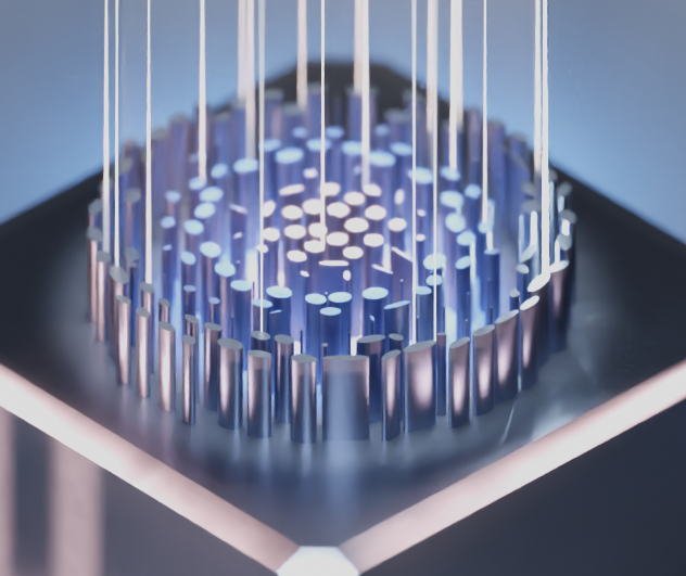
abstract = {We present a general strategy for the inverse design of metasurfaces composed of elementary shapes. We use it to design a structure that collects and collimates light from nitrogen-vacancy centers in diamond. Such metasurfaces constitute scalable optical interfaces for solid-state qubits, enabling efficient photon coupling into optical fibers and eliminating free-space collection optics. The many-body shape optimization strategy is a practical alternative to topology optimization that explicitly enforces material and fabrication constraints throughout the optimization, while still achieving high performance. The metasurface is easily adaptable to other solid-state qubits, and the optimization method is broadly applicable to fabrication-constrained photonic design problems.},
keywords = {diamond fabrication, diamond NV center, Nanophotonics, photoluminescence},
pubstate = {published},
tppubtype = {article}
}
Brown, K. J.; Chartier, E.; Sweet, E. M.; A.Hopper, D.; Bassett, L. C.
Cleaning diamond surfaces using boiling acid treatment in a standard laboratory chemical hood Journal Article
In: Journal of Chemical Health and Safety, vol. 26, pp. 40-44, 2019.
Abstract | Links | BibTeX | Tags: diamond fabrication
@article{Brown2019,
title = {Cleaning diamond surfaces using boiling acid treatment in a standard laboratory chemical hood},
author = {K. J. Brown and E. Chartier and E. M. Sweet and D. A.Hopper and L. C. Bassett},
url = {https://pubs.acs.org/doi/10.1021/acs.chas.8b26611},
year = {2019},
date = {2019-11-01},
journal = {Journal of Chemical Health and Safety},
volume = {26},
pages = {40-44},
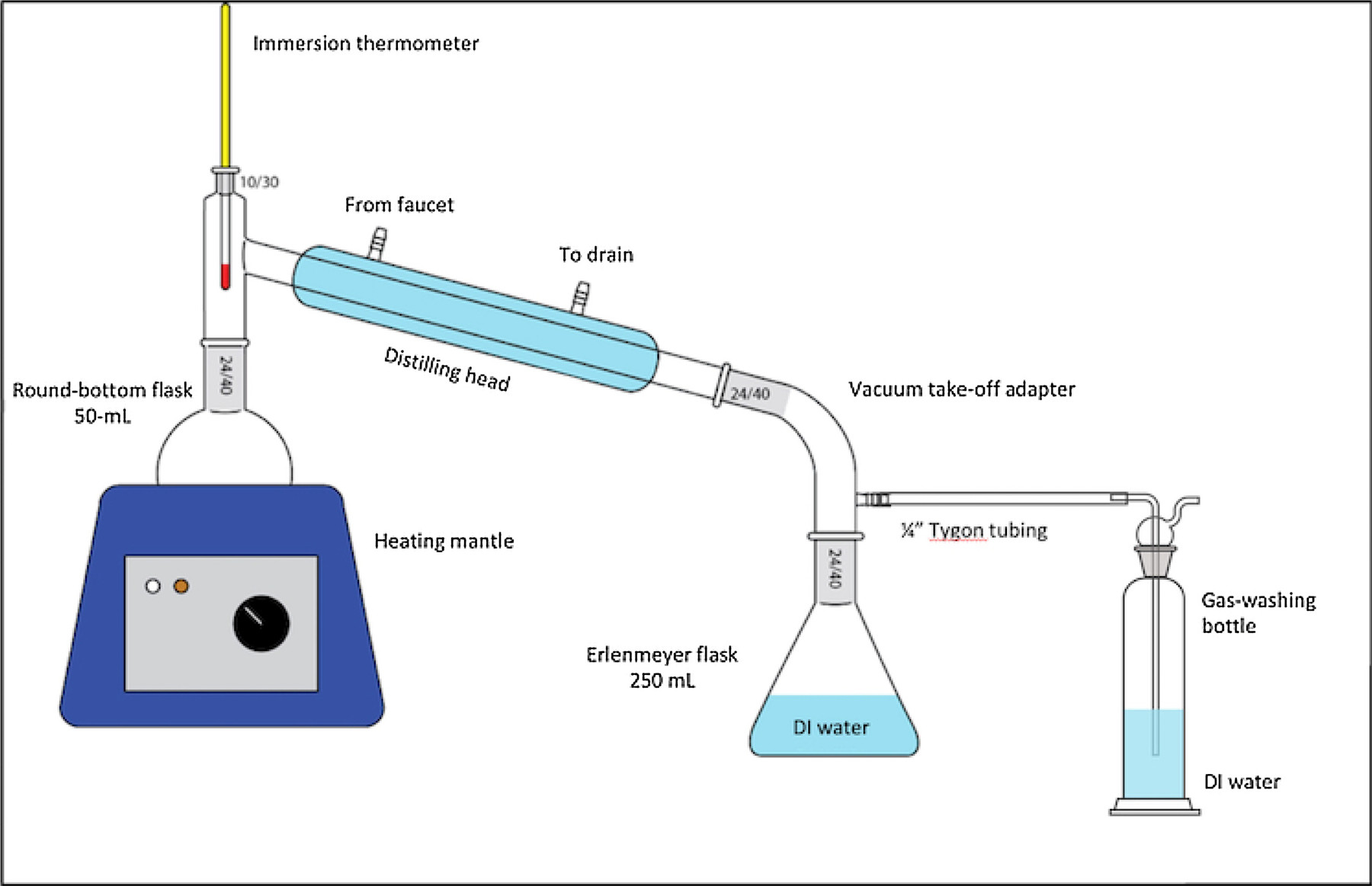
abstract = {Diamond is the basis for numerous applications in optics, electronics, and quantum science due to its desirable material properties and the existence of optically active spins such as the nitrogen-vacancy (NV) center. For some applications, pristine diamond surfaces are required. However, treatments such as irradiation and high-temperature annealing used to create NV centers produce unwanted graphitic and pyrolytic domains of carbon that are difficult to remove using most chemical treatments. A boiling mixture of nitric, perchloric, and sulfuric acids is known to selectively etch graphitic carbon and is commonly used in the research community to restore a clean diamond surface. The risks associated with using these acids, in the presence of organic material, are explosion due to the potential creation of perchlorate salts, as well as ignition due to the presence of an oxygen source from all three acids and a fuel source from the organic material. In this paper, we will discuss a method that mitigates these risks of the cleaning process without requiring a special laboratory chemical hood with a wash-down feature. This method was brought to the attention of health and safety staff after a research group at The University of Pennsylvania requested information about the safety of the procedure and preventative controls.},
keywords = {diamond fabrication},
pubstate = {published},
tppubtype = {article}
}
Huang, T -Y; Grote, R R; Mann, S A; Hopper, D A; Exarhos, A L; Lopez, G G; Klein, A R; Garnett, E C; Bassett, L C
Imaging a nitrogen-vacancy center with a diamond immersion metalens Journal Article
In: Nature Communications, vol. 10, no. 2392, 2019.
Abstract | Links | BibTeX | Tags: diamond fabrication, Nanophotonics
@article{Huang2019,
title = {Imaging a nitrogen-vacancy center with a diamond immersion metalens},
author = {T -Y Huang and R R Grote and S A Mann and D A Hopper and A L Exarhos and G G Lopez and A R Klein and E C Garnett and L C Bassett},
url = {https://www.nature.com/articles/s41467-019-10238-5
https://medium.com/penn-engineering/penn-engineers-design-nanostructured-diamond-metalens-for-compact-quantum-technologies-271adddf69ba},
year = {2019},
date = {2019-06-03},
journal = {Nature Communications},
volume = {10},
number = {2392},
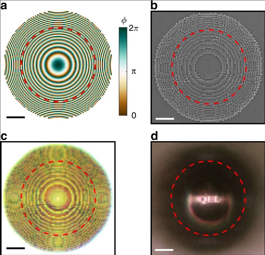
abstract = {Quantum emitters such as the diamond nitrogen-vacancy (NV) center are the basis for a wide range of quantum technologies. However, refraction and reflections at material interfaces impede photon collection, and the emitters’ atomic scale necessitates the use of free space optical measurement setups that prevent packaging of quantum devices. To overcome these limitations, we design and fabricate a metasurface composed of nanoscale diamond pillars that acts as an immersion lens to collect and collimate the emission of an individual NV center. The metalens exhibits a numerical aperture greater than 1.0, enabling efficient fiber-coupling of quantum emitters. This flexible design will lead to the miniaturization of quantum devices in a wide range of host materials and the development of metasurfaces that shape single-photon emission for coupling to optical cavities or route photons based on their quantum state.},
keywords = {diamond fabrication, Nanophotonics},
pubstate = {published},
tppubtype = {article}
}
Parks, S M; Grote, R R; Hopper, D A; Bassett, L C
Fabrication of (111)-faced single-crystal diamond plates by laser nucleated cleaving Journal Article
In: Diamond and Related Materials, vol. 84, pp. 20-25, 2018.
Abstract | Links | BibTeX | Tags: diamond fabrication
@article{Parks2018,
title = {Fabrication of (111)-faced single-crystal diamond plates by laser nucleated cleaving},
author = {S M Parks and R R Grote and D A Hopper and L C Bassett},
url = {https://www.sciencedirect.com/science/article/pii/S0925963517307136?via%3Dihub
https://arxiv.org/abs/1712.03882},
year = {2018},
date = {2018-02-28},
journal = {Diamond and Related Materials},
volume = {84},
pages = {20-25},
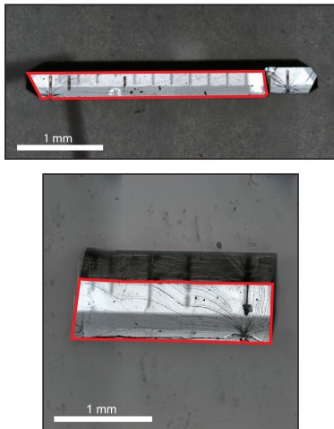
abstract = {Single-crystal diamond plates with surfaces oriented in a (111) crystal plane are required for high-performance solid-state device platforms ranging from power electronics to quantum information processing architectures. However, producing plates with this orientation has proven challenging. In this paper, we demonstrate a method for reliably and precisely fabricating (111)-faced plates from commercially available, chemical-vapor-deposition-grown, type-IIa single-crystal diamond substrates with (100) faces. Our method uses a nanosecond-pulsed visible laser to nucleate and propagate a mechanical cleave in a chosen (111) crystal plane, resulting in faces as large as 3.0mm × 0.3mm with atomically flat surfaces, negligible miscut angles, and near zero kerf loss. We discuss the underlying physical mechanisms of the process along with potential improvements that will enable the production of millimeter-scale (111)-faced single-crystal diamond plates for a variety of emerging devices and applications.},
keywords = {diamond fabrication},
pubstate = {published},
tppubtype = {article}
}
Grote, R R; Bassett, L C
Single-mode optical waveguides on native high-refractive-index substrates Journal Article
In: APL Photonics, vol. 1, pp. 071302, 2016.
Abstract | Links | BibTeX | Tags: diamond fabrication, Nanophotonics
@article{Grote2016,
title = {Single-mode optical waveguides on native high-refractive-index substrates},
author = {R R Grote and L C Bassett},
url = {https://aip.scitation.org/doi/10.1063/1.4955065},
year = {2016},
date = {2016-08-01},
journal = {APL Photonics},
volume = {1},
pages = {071302},
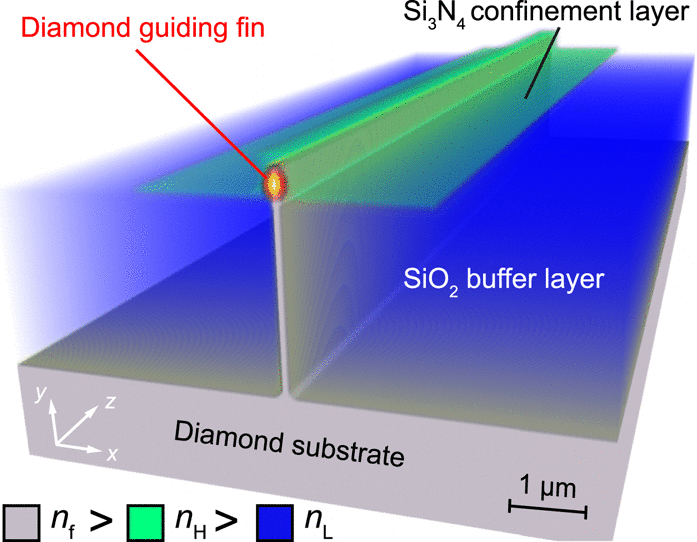
abstract = {High-refractive-index semiconductor optical waveguides form the basis for modern photonic integrated circuits (PICs). However, conventional methods for achieving optical confinement require a thick lower-refractive-index support layer that impedes large-scale co-integration with electronics and limits the materials on which PICs can be fabricated. To address this challenge, we present a general architecture for single-mode waveguides that confine light in a high-refractive-index material on a native substrate. The waveguide consists of a high-aspect-ratio fin of the guiding material surrounded by lower-refractive-index dielectrics and is compatible with standard top-down fabrication techniques. This letter describes a physically intuitive, semi-analytical, effective index model for designing fin waveguides, which is confirmed with fully vectorial numerical simulations. Design examples are presented for diamond and silicon at visible and telecommunications wavelengths, respectively, along with calculations of propagation loss due to bending, scattering, and substrate leakage. Potential methods of fabrication are also discussed. The proposed waveguide geometry allows PICs to be fabricated alongside silicon CMOS electronics on the same wafer, removes the need for heteroepitaxy in III-V PICs, and will enable wafer-scale photonic integration on emerging material platforms such as diamond and SiC.},
keywords = {diamond fabrication, Nanophotonics},
pubstate = {published},
tppubtype = {article}
}
2024
Klein, Amelia R.; Engheta, Nader; Bassett, Lee C.
Designing metasurface optical interfaces for solid-state qubits using many-body adjoint shape optimization Journal Article
In: Optics Express, vol. 32, iss. 22, pp. 38504-38515, 2024.
@article{Klein2024,

title = {Designing metasurface optical interfaces for solid-state qubits using many-body adjoint shape optimization},

author = {Amelia R. Klein and Nader Engheta and Lee C. Bassett},

url = {https://opg.optica.org/oe/fulltext.cfm?uri=oe-32-22-38504&id=561330

https://arxiv.org/abs/2406.08212},

doi = {10.1364/OE.522501},

year  = {2024},

date = {2024-10-09},

urldate = {2024-10-09},

journal = {Optics Express},

volume = {32},

issue = {22},

pages = {38504-38515},

abstract = {We present a general strategy for the inverse design of metasurfaces composed of elementary shapes. We use it to design a structure that collects and collimates light from nitrogen-vacancy centers in diamond. Such metasurfaces constitute scalable optical interfaces for solid-state qubits, enabling efficient photon coupling into optical fibers and eliminating free-space collection optics. The many-body shape optimization strategy is a practical alternative to topology optimization that explicitly enforces material and fabrication constraints throughout the optimization, while still achieving high performance. The metasurface is easily adaptable to other solid-state qubits, and the optimization method is broadly applicable to fabrication-constrained photonic design problems.},

keywords = {},

pubstate = {published},

tppubtype = {article}

}
2019
Brown, K. J.; Chartier, E.; Sweet, E. M.; A.Hopper, D.; Bassett, L. C.
Cleaning diamond surfaces using boiling acid treatment in a standard laboratory chemical hood Journal Article
In: Journal of Chemical Health and Safety, vol. 26, pp. 40-44, 2019.
@article{Brown2019,

title = {Cleaning diamond surfaces using boiling acid treatment in a standard laboratory chemical hood},

author = {K. J. Brown and E. Chartier and E. M. Sweet and D. A.Hopper and L. C. Bassett},

url = {https://pubs.acs.org/doi/10.1021/acs.chas.8b26611},

year  = {2019},

date = {2019-11-01},

journal = {Journal of Chemical Health and Safety},

volume = {26},

pages = {40-44},

abstract = {Diamond is the basis for numerous applications in optics, electronics, and quantum science due to its desirable material properties and the existence of optically active spins such as the nitrogen-vacancy (NV) center. For some applications, pristine diamond surfaces are required. However, treatments such as irradiation and high-temperature annealing used to create NV centers produce unwanted graphitic and pyrolytic domains of carbon that are difficult to remove using most chemical treatments. A boiling mixture of nitric, perchloric, and sulfuric acids is known to selectively etch graphitic carbon and is commonly used in the research community to restore a clean diamond surface. The risks associated with using these acids, in the presence of organic material, are explosion due to the potential creation of perchlorate salts, as well as ignition due to the presence of an oxygen source from all three acids and a fuel source from the organic material. In this paper, we will discuss a method that mitigates these risks of the cleaning process without requiring a special laboratory chemical hood with a wash-down feature. This method was brought to the attention of health and safety staff after a research group at The University of Pennsylvania requested information about the safety of the procedure and preventative controls.},

keywords = {},

pubstate = {published},

tppubtype = {article}

}
Huang, T -Y; Grote, R R; Mann, S A; Hopper, D A; Exarhos, A L; Lopez, G G; Klein, A R; Garnett, E C; Bassett, L C
Imaging a nitrogen-vacancy center with a diamond immersion metalens Journal Article
In: Nature Communications, vol. 10, no. 2392, 2019.
@article{Huang2019,

title = {Imaging a nitrogen-vacancy center with a diamond immersion metalens},

author = {T -Y Huang and R R Grote and S A Mann and D A Hopper and A L Exarhos and G G Lopez and A R Klein and E C Garnett and L C Bassett},

url = {https://www.nature.com/articles/s41467-019-10238-5

https://medium.com/penn-engineering/penn-engineers-design-nanostructured-diamond-metalens-for-compact-quantum-technologies-271adddf69ba},

year  = {2019},

date = {2019-06-03},

journal = {Nature Communications},

volume = {10},

number = {2392},

abstract = {Quantum emitters such as the diamond nitrogen-vacancy (NV) center are the basis for a wide range of quantum technologies. However, refraction and reflections at material interfaces impede photon collection, and the emitters’ atomic scale necessitates the use of free space optical measurement setups that prevent packaging of quantum devices. To overcome these limitations, we design and fabricate a metasurface composed of nanoscale diamond pillars that acts as an immersion lens to collect and collimate the emission of an individual NV center. The metalens exhibits a numerical aperture greater than 1.0, enabling efficient fiber-coupling of quantum emitters. This flexible design will lead to the miniaturization of quantum devices in a wide range of host materials and the development of metasurfaces that shape single-photon emission for coupling to optical cavities or route photons based on their quantum state.},

keywords = {},

pubstate = {published},

tppubtype = {article}

}
2018
Parks, S M; Grote, R R; Hopper, D A; Bassett, L C
Fabrication of (111)-faced single-crystal diamond plates by laser nucleated cleaving Journal Article
In: Diamond and Related Materials, vol. 84, pp. 20-25, 2018.
@article{Parks2018,

title = {Fabrication of (111)-faced single-crystal diamond plates by laser nucleated cleaving},

author = {S M Parks and R R Grote and D A Hopper and L C Bassett},

url = {https://www.sciencedirect.com/science/article/pii/S0925963517307136?via%3Dihub


https://arxiv.org/abs/1712.03882},

year  = {2018},

date = {2018-02-28},

journal = {Diamond and Related Materials},

volume = {84},

pages = {20-25},

abstract = {Single-crystal diamond plates with surfaces oriented in a (111) crystal plane are required for high-performance solid-state device platforms ranging from power electronics to quantum information processing architectures. However, producing plates with this orientation has proven challenging. In this paper, we demonstrate a method for reliably and precisely fabricating (111)-faced plates from commercially available, chemical-vapor-deposition-grown, type-IIa single-crystal diamond substrates with (100) faces. Our method uses a nanosecond-pulsed visible laser to nucleate and propagate a mechanical cleave in a chosen (111) crystal plane, resulting in faces as large as 3.0mm × 0.3mm with atomically flat surfaces, negligible miscut angles, and near zero kerf loss. We discuss the underlying physical mechanisms of the process along with potential improvements that will enable the production of millimeter-scale (111)-faced single-crystal diamond plates for a variety of emerging devices and applications.},

keywords = {},

pubstate = {published},

tppubtype = {article}

}
2016
Grote, R R; Bassett, L C
Single-mode optical waveguides on native high-refractive-index substrates Journal Article
In: APL Photonics, vol. 1, pp. 071302, 2016.
@article{Grote2016,

title = {Single-mode optical waveguides on native high-refractive-index substrates},

author = {R R Grote and L C Bassett},

url = {https://aip.scitation.org/doi/10.1063/1.4955065},

year  = {2016},

date = {2016-08-01},

journal = {APL Photonics},

volume = {1},

pages = {071302},

abstract = {High-refractive-index semiconductor optical waveguides form the basis for modern photonic integrated circuits (PICs). However, conventional methods for achieving optical confinement require a thick lower-refractive-index support layer that impedes large-scale co-integration with electronics and limits the materials on which PICs can be fabricated. To address this challenge, we present a general architecture for single-mode waveguides that confine light in a high-refractive-index material on a native substrate. The waveguide consists of a high-aspect-ratio fin of the guiding material surrounded by lower-refractive-index dielectrics and is compatible with standard top-down fabrication techniques. This letter describes a physically intuitive, semi-analytical, effective index model for designing fin waveguides, which is confirmed with fully vectorial numerical simulations. Design examples are presented for diamond and silicon at visible and telecommunications wavelengths, respectively, along with calculations of propagation loss due to bending, scattering, and substrate leakage. Potential methods of fabrication are also discussed. The proposed waveguide geometry allows PICs to be fabricated alongside silicon CMOS electronics on the same wafer, removes the need for heteroepitaxy in III-V PICs, and will enable wafer-scale photonic integration on emerging material platforms such as diamond and SiC.},

keywords = {},

pubstate = {published},

tppubtype = {article}

}
Select publications before 2014
- “All-optical control of a solid-state spin using coherent dark states”, C. G. Yale, B. B. Buckley, D. J. Christle, G. Burkard, F. J. Heremans, L. C. Bassett, and D. D. Awschalom, Proc. Natl. Acad. Sci. USA 110, 7595 (2013).
- “Quantum spintronics: Engineering and manipulating atom-like spins in semiconductors”, D.D. Awschalom, L.C. Bassett, A.S. Dzurak, E.L. Hu and J.R. Petta, Science 339, 1174 (2013).
Related article: “The Future of Quantum Information Processing”, J. Stajic, Science 339, 1163 (2013).
- “Engineering and quantum control of single spins in semiconductors”, D.M. Toyli, L.C. Bassett, B.B. Buckley, G. Calusine and D.D. Awschalom, MRS Bulletin 38, 139 (2013).
- “Engineering shallow spins in diamond with nitrogen delta-doping”, K. Ohno, F. J. Heremans, L. C. Bassett, B. A. Myers, D. M. Toyli, A. C. Bleszynski-Jayich, C. J. Palmstrøm, and D. D. Awschalom, Appl. Phys. Lett. 101, 082413 (2012).
- “Electrical tuning of single nitrogen-vacancy center optical transitions enhanced by photoinduced fields”, L. C. Bassett, F. J. Heremans, C. G. Yale, B. B. Buckley, and D. D. Awschalom, Phys. Rev. Lett. 107, 266403 (2011).
- “Spin-light coherence for single-spin measurement and control in diamond”, B. B. Buckley, G. D. Fuchs, L. C. Bassett, and D. D. Awschalom, Science 330, 1212 (2010).
Related article: “Quantum measurement and control of single spins in diamond”, Science 330, 1188 (2010).