
Bassett, L. C.; Alkauskas, A.; Exarhos, A. L.; Fu, K. -M. C.
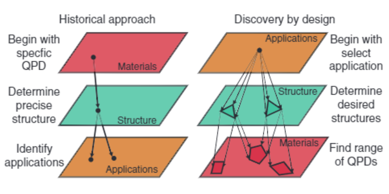
Quantum defects by design Journal Article
In: Nanophotonics, vol. 8, no. 11, 2019.
Abstract | Links | BibTeX | Tags: Nanophotonics, optical sources, point defects, Quantum Control
@article{Bassett2019b,

title = {Quantum defects by design},

author = {L. C. Bassett and A. Alkauskas and A. L. Exarhos and K.-M. C. Fu},

url = {https://www.degruyter.com/view/journals/nanoph/8/11/article-p1867.xml},

year  = {2019},

date = {2019-10-04},

journal = {Nanophotonics},

volume = {8},

number = {11},

abstract = {Part of Special Issue on Quantum Nanophotonics in Emerging Materials.


Miniaturization of electronic and opto-electronic semiconductor devices has been happening ever since the first such devices appeared. Eventually, one can envision a device that is composed of just a few atoms. As these atoms ideally should not float in free space, but should be embedded in a solid-state matrix, this naturally brings one to the concept of a point defect (an impurity atom or complex of atoms) as the ultimate electronic or opto-electronic device. At such tiny length scales the behavior of physical systems is governed by the laws of quantum mechanics. Therefore, it is no surprise that an increasing number of point defects are being considered as building blocks for various applications in the field of quantum information science; more specifically, in quantum sensing, quantum communication, and quantum computing [1], [2], [3], [4]. We refer to these desirable defects as quantum point defects (QPDs). Prominent examples include the nitrogen-vacancy (NV) center in diamond, the silicon-vacancy (SiV) center in diamond, the divacancy in silicon carbide, and rare-earth impurities in complex oxides.},

keywords = {Nanophotonics, optical sources, point defects, Quantum Control},

pubstate = {published},

tppubtype = {article}

}
Miniaturization of electronic and opto-electronic semiconductor devices has been happening ever since the first such devices appeared. Eventually, one can envision a device that is composed of just a few atoms. As these atoms ideally should not float in free space, but should be embedded in a solid-state matrix, this naturally brings one to the concept of a point defect (an impurity atom or complex of atoms) as the ultimate electronic or opto-electronic device. At such tiny length scales the behavior of physical systems is governed by the laws of quantum mechanics. Therefore, it is no surprise that an increasing number of point defects are being considered as building blocks for various applications in the field of quantum information science; more specifically, in quantum sensing, quantum communication, and quantum computing [1], [2], [3], [4]. We refer to these desirable defects as quantum point defects (QPDs). Prominent examples include the nitrogen-vacancy (NV) center in diamond, the silicon-vacancy (SiV) center in diamond, the divacancy in silicon carbide, and rare-earth impurities in complex oxides.
Turiansky, M E; Alkauskas, A; Bassett, L C; de Walle, Van C G
Dangling bonds in hexagonal boron nitride as single-photon emitters Journal Article
In: Physical Review Letters, vol. 123, no. 12, pp. 127401, 2019, ISSN: 1079-7114.
Abstract | Links | BibTeX | Tags: 2-dimensional systems, Condensed Matter, First-principles calculations, Optical absorption spectroscopy, Optical microcavities, optical sources, point defects, Quantum wells, Semiconductor compounds
@article{Turiansky2019,
title = {Dangling bonds in hexagonal boron nitride as single-photon emitters},
author = {M E Turiansky and A Alkauskas and L C Bassett and Van C G de Walle},
url = {https://journals.aps.org/prl/abstract/10.1103/PhysRevLett.123.127401},
doi = {10.1103},
issn = {1079-7114},
year = {2019},
date = {2019-09-16},
journal = {Physical Review Letters},
volume = {123},
number = {12},
pages = {127401},
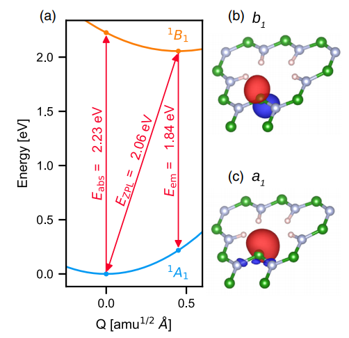
abstract = {Hexagonal boron nitride has been found to host color centers that exhibit single-photon emission, but the microscopic origin of these emitters is unknown. We propose boron dangling bonds as the likely source of the observed single-photon emission around 2 eV. An optical transition where an electron is excited from a doubly occupied boron dangling bond to a localized B pz state gives rise to a zero-phonon line of 2.06 eV and emission with a Huang-Rhys factor of 2.3. This transition is linearly polarized with the absorptive and emissive dipole aligned. Because of the energetic position of the states within the band gap, indirect excitation through the conduction band will occur for sufficiently large excitation energies, leading to the misalignment of the absorptive and emissive dipoles seen in experiment. Our calculations predict a singlet ground state and the existence of a metastable triplet state, in agreement with experiment.},
keywords = {2-dimensional systems, Condensed Matter, First-principles calculations, Optical absorption spectroscopy, Optical microcavities, optical sources, point defects, Quantum wells, Semiconductor compounds},
pubstate = {published},
tppubtype = {article}
}
Exarhos, A L; Hopper, D A; Grote, R R; Alkauskas, A; Bassett, L C
Optical signatures of quantum emitters in suspended hexagonal boron nitride Journal Article
In: ACS Nano, vol. 11, pp. 3328-3336, 2017.
Abstract | Links | BibTeX | Tags: 2-dimensional systems, Condensed Matter, optical sources, point defects
@article{Exarhos2017,
title = {Optical signatures of quantum emitters in suspended hexagonal boron nitride},
author = {A L Exarhos and D A Hopper and R R Grote and A Alkauskas and L C Bassett},
url = {https://pubs.acs.org/doi/abs/10.1021/acsnano.7b00665},
year = {2017},
date = {2017-03-07},
journal = {ACS Nano},
volume = {11},
pages = {3328-3336},
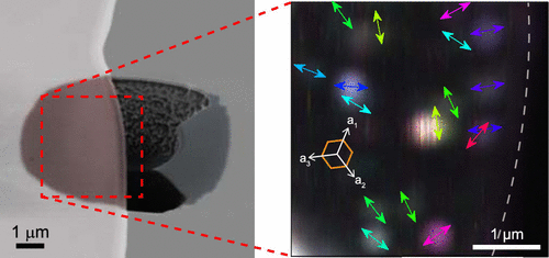
abstract = {Hexagonal boron nitride (h-BN) is rapidly emerging as an attractive material for solid-state quantum engineering. Analogously to three-dimensional wide-band-gap semiconductors such as diamond, h-BN hosts isolated defects exhibiting visible fluorescence at room temperature, and the ability to position such quantum emitters within a two-dimensional material promises breakthrough advances in quantum sensing, photonics, and other quantum technologies. Critical to such applications is an understanding of the physics underlying h-BN’s quantum emission. We report the creation and characterization of visible single-photon sources in suspended, single-crystal, h-BN films. With substrate interactions eliminated, we study the spectral, temporal, and spatial characteristics of the defects’ optical emission. Theoretical analysis of the defects’ spectra reveals similarities in vibronic coupling to h-BN phonon modes despite widely varying fluorescence wavelengths, and a statistical analysis of the polarized emission from many emitters throughout the same single-crystal flake uncovers a weak correlation between the optical dipole orientations of some defects and h-BN’s primitive crystallographic axes, despite a clear misalignment for other dipoles. These measurements constrain possible defect models and, moreover, suggest that several classes of emitters can exist simultaneously throughout free-standing h-BN, whether they be different defects, different charge states of the same defect, or the result of strong local perturbations.},
keywords = {2-dimensional systems, Condensed Matter, optical sources, point defects},
pubstate = {published},
tppubtype = {article}
}
2019
Bassett, L. C.; Alkauskas, A.; Exarhos, A. L.; Fu, K. -M. C.
Quantum defects by design Journal Article
In: Nanophotonics, vol. 8, no. 11, 2019.
@article{Bassett2019b,

title = {Quantum defects by design},

author = {L. C. Bassett and A. Alkauskas and A. L. Exarhos and K.-M. C. Fu},

url = {https://www.degruyter.com/view/journals/nanoph/8/11/article-p1867.xml},

year  = {2019},

date = {2019-10-04},

journal = {Nanophotonics},

volume = {8},

number = {11},

abstract = {Part of Special Issue on Quantum Nanophotonics in Emerging Materials.


Miniaturization of electronic and opto-electronic semiconductor devices has been happening ever since the first such devices appeared. Eventually, one can envision a device that is composed of just a few atoms. As these atoms ideally should not float in free space, but should be embedded in a solid-state matrix, this naturally brings one to the concept of a point defect (an impurity atom or complex of atoms) as the ultimate electronic or opto-electronic device. At such tiny length scales the behavior of physical systems is governed by the laws of quantum mechanics. Therefore, it is no surprise that an increasing number of point defects are being considered as building blocks for various applications in the field of quantum information science; more specifically, in quantum sensing, quantum communication, and quantum computing [1], [2], [3], [4]. We refer to these desirable defects as quantum point defects (QPDs). Prominent examples include the nitrogen-vacancy (NV) center in diamond, the silicon-vacancy (SiV) center in diamond, the divacancy in silicon carbide, and rare-earth impurities in complex oxides.},

keywords = {},

pubstate = {published},

tppubtype = {article}

}
Miniaturization of electronic and opto-electronic semiconductor devices has been happening ever since the first such devices appeared. Eventually, one can envision a device that is composed of just a few atoms. As these atoms ideally should not float in free space, but should be embedded in a solid-state matrix, this naturally brings one to the concept of a point defect (an impurity atom or complex of atoms) as the ultimate electronic or opto-electronic device. At such tiny length scales the behavior of physical systems is governed by the laws of quantum mechanics. Therefore, it is no surprise that an increasing number of point defects are being considered as building blocks for various applications in the field of quantum information science; more specifically, in quantum sensing, quantum communication, and quantum computing [1], [2], [3], [4]. We refer to these desirable defects as quantum point defects (QPDs). Prominent examples include the nitrogen-vacancy (NV) center in diamond, the silicon-vacancy (SiV) center in diamond, the divacancy in silicon carbide, and rare-earth impurities in complex oxides.
Turiansky, M E; Alkauskas, A; Bassett, L C; de Walle, Van C G
Dangling bonds in hexagonal boron nitride as single-photon emitters Journal Article
In: Physical Review Letters, vol. 123, no. 12, pp. 127401, 2019, ISSN: 1079-7114.
@article{Turiansky2019,

title = {Dangling bonds in hexagonal boron nitride as single-photon emitters},

author = {M E Turiansky and A Alkauskas and L C Bassett and Van C G de Walle},

url = {https://journals.aps.org/prl/abstract/10.1103/PhysRevLett.123.127401},

doi = {10.1103},

issn = {1079-7114},

year  = {2019},

date = {2019-09-16},

journal = {Physical Review Letters},

volume = {123},

number = {12},

pages = {127401},

abstract = {Hexagonal boron nitride has been found to host color centers that exhibit single-photon emission, but the microscopic origin of these emitters is unknown. We propose boron dangling bonds as the likely source of the observed single-photon emission around 2 eV. An optical transition where an electron is excited from a doubly occupied boron dangling bond to a localized B pz state gives rise to a zero-phonon line of 2.06 eV and emission with a Huang-Rhys factor of 2.3. This transition is linearly polarized with the absorptive and emissive dipole aligned. Because of the energetic position of the states within the band gap, indirect excitation through the conduction band will occur for sufficiently large excitation energies, leading to the misalignment of the absorptive and emissive dipoles seen in experiment. Our calculations predict a singlet ground state and the existence of a metastable triplet state, in agreement with experiment.},

keywords = {},

pubstate = {published},

tppubtype = {article}

}
2017
Exarhos, A L; Hopper, D A; Grote, R R; Alkauskas, A; Bassett, L C
Optical signatures of quantum emitters in suspended hexagonal boron nitride Journal Article
In: ACS Nano, vol. 11, pp. 3328-3336, 2017.
@article{Exarhos2017,

title = {Optical signatures of quantum emitters in suspended hexagonal boron nitride},

author = {A L Exarhos and D A Hopper and R R Grote and A Alkauskas and L C Bassett},

url = {https://pubs.acs.org/doi/abs/10.1021/acsnano.7b00665},

year  = {2017},

date = {2017-03-07},

journal = {ACS Nano},

volume = {11},

pages = {3328-3336},

abstract = {Hexagonal boron nitride (h-BN) is rapidly emerging as an attractive material for solid-state quantum engineering. Analogously to three-dimensional wide-band-gap semiconductors such as diamond, h-BN hosts isolated defects exhibiting visible fluorescence at room temperature, and the ability to position such quantum emitters within a two-dimensional material promises breakthrough advances in quantum sensing, photonics, and other quantum technologies. Critical to such applications is an understanding of the physics underlying h-BN’s quantum emission. We report the creation and characterization of visible single-photon sources in suspended, single-crystal, h-BN films. With substrate interactions eliminated, we study the spectral, temporal, and spatial characteristics of the defects’ optical emission. Theoretical analysis of the defects’ spectra reveals similarities in vibronic coupling to h-BN phonon modes despite widely varying fluorescence wavelengths, and a statistical analysis of the polarized emission from many emitters throughout the same single-crystal flake uncovers a weak correlation between the optical dipole orientations of some defects and h-BN’s primitive crystallographic axes, despite a clear misalignment for other dipoles. These measurements constrain possible defect models and, moreover, suggest that several classes of emitters can exist simultaneously throughout free-standing h-BN, whether they be different defects, different charge states of the same defect, or the result of strong local perturbations.},

keywords = {},

pubstate = {published},

tppubtype = {article}

}
Select publications before 2014
- “All-optical control of a solid-state spin using coherent dark states”, C. G. Yale, B. B. Buckley, D. J. Christle, G. Burkard, F. J. Heremans, L. C. Bassett, and D. D. Awschalom, Proc. Natl. Acad. Sci. USA 110, 7595 (2013).
- “Quantum spintronics: Engineering and manipulating atom-like spins in semiconductors”, D.D. Awschalom, L.C. Bassett, A.S. Dzurak, E.L. Hu and J.R. Petta, Science 339, 1174 (2013).
Related article: “The Future of Quantum Information Processing”, J. Stajic, Science 339, 1163 (2013).
- “Engineering and quantum control of single spins in semiconductors”, D.M. Toyli, L.C. Bassett, B.B. Buckley, G. Calusine and D.D. Awschalom, MRS Bulletin 38, 139 (2013).
- “Engineering shallow spins in diamond with nitrogen delta-doping”, K. Ohno, F. J. Heremans, L. C. Bassett, B. A. Myers, D. M. Toyli, A. C. Bleszynski-Jayich, C. J. Palmstrøm, and D. D. Awschalom, Appl. Phys. Lett. 101, 082413 (2012).
- “Electrical tuning of single nitrogen-vacancy center optical transitions enhanced by photoinduced fields”, L. C. Bassett, F. J. Heremans, C. G. Yale, B. B. Buckley, and D. D. Awschalom, Phys. Rev. Lett. 107, 266403 (2011).
- “Spin-light coherence for single-spin measurement and control in diamond”, B. B. Buckley, G. D. Fuchs, L. C. Bassett, and D. D. Awschalom, Science 330, 1212 (2010).
Related article: “Quantum measurement and control of single spins in diamond”, Science 330, 1188 (2010).