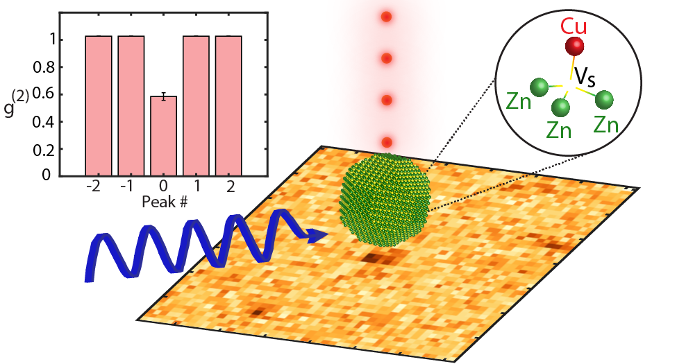
Panfil, Yossef E.; Thompson, Sarah M.; Chen, Gary; Ng, Jonah; Kagan, Cherie R.; Bassett, Lee C.
Room-temperature quantum emission from CuZn-VS defects in ZnS:Cu colloidal nanocrystals Journal Article Forthcoming
In: ACS Nano, Forthcoming.
Abstract | Links | BibTeX | Tags: colloidal nanocrystals, forthcoming, quantum defects, ZnS
@article{Panfil2025,

title = {Room-temperature quantum emission from CuZn-VS defects in ZnS:Cu colloidal nanocrystals},

author = {Yossef E. Panfil and Sarah M. Thompson and Gary Chen and Jonah Ng and Cherie R. Kagan and Lee C. Bassett},

url = {https://pubs.acs.org/doi/abs/10.1021/acsnano.5c01265

https://arxiv.org/abs/2501.11812},

year  = {2025},

date = {2025-06-05},

urldate = {2025-01-21},

journal = {ACS Nano},

abstract = {We report room-temperature observations of CuZn-VS quantum emitters in individual ZnS:Cu nanocrystals (NCs). Using time-gated imaging, we isolate the distinct, ∼3-μs-long, red photoluminescence (PL) emission of CuZn-VS defects, enabling their precise identification and statistical characterization. The emitters exhibit distinct blinking and photon antibunching, consistent with individual NCs containing two to four CuZn-VS defects. The quantum emitters' PL spectra show a pronounced blue shift compared to NC dispersions, likely due to photochemical and charging effects. Emission polarization measurements of quantum emitters are consistent with a σ-character optical dipole transition and the symmetry of the CuZn-VS defect. These observations motivate further investigation of CuZn-VS defects in ZnS NCs for use in quantum technologies.},

keywords = {colloidal nanocrystals, forthcoming, quantum defects, ZnS},

pubstate = {forthcoming},

tppubtype = {article}

}
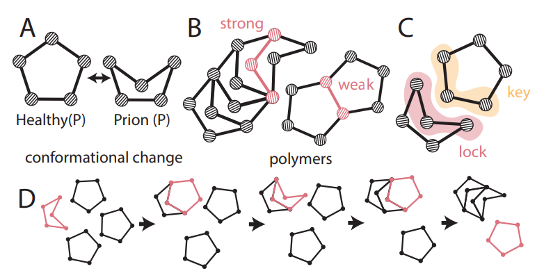
Ouellet, Mathieu; Bassett, Dani S.; Bassett, Lee C.; Murphy, Kieran A.; Patankar, Shubhankar P.
Mechanical prions as self-assembling microstructures Journal Article Forthcoming
In: Newton, Forthcoming.
Abstract | Links | BibTeX | Tags: complex systems, forthcoming
@article{Ouellet2025,

title = {Mechanical prions as self-assembling microstructures},

author = {Mathieu Ouellet and Dani S. Bassett and Lee C. Bassett and Kieran A. Murphy and Shubhankar P. Patankar},

url = {https://www.cell.com/newton/fulltext/S2950-6360(25)00090-8

https://arxiv.org/abs/2402.10939},

year  = {2025},

date = {2025-05-08},

urldate = {2024-04-16},

journal = {Newton},

abstract = {Prions are misfolded proteins that transmit their structural arrangement to neighboring proteins. In biological systems, prion dynamics can produce a variety of complex functional outcomes. Yet, an understanding of prionic causes has been hampered by the fact that few computational models exist that allow for experimental design, hypothesis testing, and control. Here, we identify essential prionic properties and present a biologically inspired model of prions using simple mechanical structures capable of undergoing complex conformational change. We demonstrate the utility of our approach by designing a prototypical mechanical prion and validating its properties experimentally. Our work provides a design framework for harnessing and manipulating prionic properties in natural and artificial systems.},

keywords = {complex systems, forthcoming},

pubstate = {forthcoming},

tppubtype = {article}

}
2025
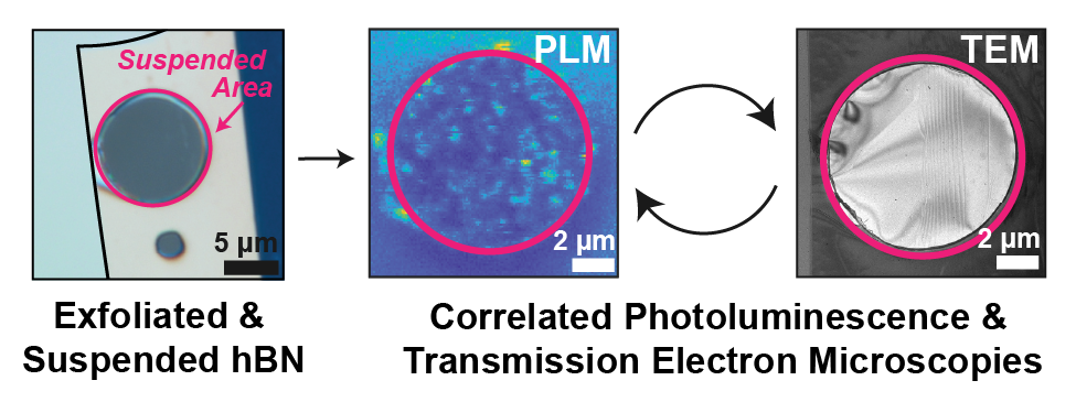
Gusdorff, Jordan A.; Bhatia, Pia; Shin, Trey T.; Uy-Tioco, Alexandra Sofia; Sailors, Benjamin N.; Keneipp, Rachael N.; Drndić, Marija; Bassett, Lee C.
Correlated Structural and Optical Characterization of Hexagonal Boron Nitride Journal Article
In: ACS Nano, vol. 9, iss. 11, pp. 11100-11110, 2025.
@article{Gusdorff2025,

title = {Correlated Structural and Optical Characterization of Hexagonal Boron Nitride},

author = {Jordan A. Gusdorff and Pia Bhatia and Trey T. Shin and Alexandra Sofia Uy-Tioco and Benjamin N. Sailors and Rachael N. Keneipp and Marija Drndić and Lee C. Bassett},

url = {https://pubs.acs.org/doi/10.1021/acsnano.4c17676

https://arxiv.org/abs/2411.14408},

doi = {10.1021/acsnano.4c17676},

year  = {2025},

date = {2025-02-21},

urldate = {2025-02-21},

journal = {ACS Nano},

volume = {9},

issue = {11},

pages = {11100-11110},

abstract = {Hexagonal boron nitride (hBN) hosts quantum emitters that exhibit single-photon emission and spin-dependent fluorescence at room temperature. These features make hBN a promising platform for quantum sensing and photonics. Despite many investigations of their optical properties, the emitters' chemical structure remains unclear, as does the role of contamination at surfaces and interfaces in forming the emitters or modifying their properties. We prepare hBN samples that are compatible with both confocal photoluminescence microscopy (PL) and transmission electron microscopy (TEM), and we use those techniques to investigate correlations between fluorescent emission, flake morphology, and surface residue. We find that the microscopy techniques themselves induce changes in hBN's optical activity and residue morphology: PL measurements induce photobleaching, whereas TEM measurements alter surface residue and emission characteristics. We also study the effects of common treatments — annealing and oxygen plasma cleaning — on the structure and optical activity of hBN. The results illustrate the power and importance of correlative studies to elucidate aspects of microscopic mechanisms that influence hBN's functionality as a host for quantum emitters and spin defects.},

keywords = {},

pubstate = {published},

tppubtype = {article}

}
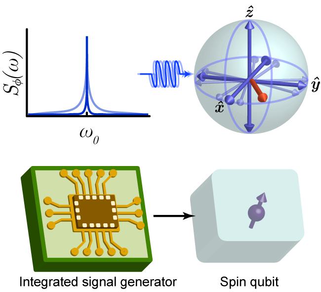
Huang, Tzu-Yung; Hopper, David A.; Omirzakhov, Kaisarbek; Idjadi, Mohamad Hossein; Breitweiser, S. Alexander; Aflatouni, Firooz; Bassett, Lee C.
Electronic Noise Considerations for Designing Integrated Solid-State Quantum Memories Journal Article
In: Advanced Quantum Technologies, pp. 2400472, 2025.
@article{Huang2025,

title = {Electronic Noise Considerations for Designing Integrated Solid-State Quantum Memories},

author = {Tzu-Yung Huang and David A. Hopper and Kaisarbek Omirzakhov and Mohamad Hossein Idjadi and S. Alexander Breitweiser and Firooz Aflatouni and Lee C. Bassett},

url = {https://onlinelibrary.wiley.com/doi/10.1002/qute.202400472#

https://arxiv.org/abs/2501.00683},

year  = {2025},

date = {2025-02-06},

urldate = {2025-02-06},

journal = {Advanced Quantum Technologies},

pages = {2400472},

abstract = {As quantum networks expand and are deployed outside research laboratories, a need arises to design and integrate compact control electronics for each memory node. It is essential to understand the performance requirements for such systems, especially concerning tolerable levels of noise, since these specifications dramatically affect a system's design complexity and cost. Here, using an approach that can be easily generalized across quantum-hardware platforms, a case study based on nitrogen-vacancy (NV) centers in diamond is presented. The effects of phase noise and timing jitter in the control system in conjunction are modeled and experimentally verified with the spin qubit's environmental noise. The impact of different phase noise characteristics on the fidelity of dynamical decoupling sequences is also considered. The results demonstrate a procedure to specify design requirements for integrated quantum control signal generators for solid-state spin qubits, depending on their coherence time, intrinsic noise spectrum, and required fidelity.},

keywords = {},

pubstate = {published},

tppubtype = {article}

}
2024
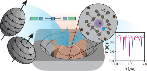
Breitweiser, S. Alex; Ouellet, Mathieu; Huang, Tzu-Yung; Taminiau, Tim H.; Bassett, Lee C.
Quadrupolar resonance spectroscopy of individual nuclei using a room-temperature quantum sensor Journal Article
In: Nano Letters, vol. 24, iss. 51, pp. 16253-16260, 2024.
@article{Breitweiser2024,

title = {Quadrupolar resonance spectroscopy of individual nuclei using a room-temperature quantum sensor},

author = {S. Alex Breitweiser and Mathieu Ouellet and Tzu-Yung Huang and Tim H. Taminiau and Lee C. Bassett},

url = {https://pubs.acs.org/doi/abs/10.1021/acs.nanolett.4c04112

https://arxiv.org/abs/2405.14859},

year  = {2024},

date = {2024-12-12},

urldate = {2024-12-12},

journal = {Nano Letters},

volume = {24},

issue = {51},

pages = {16253-16260},

abstract = {Nuclear quadrupolar resonance (NQR) spectroscopy reveals chemical bonding patterns in materials and molecules through the unique coupling between nuclear spins and local fields. However, traditional NQR techniques require macroscopic ensembles of nuclei to yield a detectable signal, which obscures molecule-to-molecule variations. Solid-state spin qubits, such as the nitrogen-vacancy (NV) center in diamond, facilitate the detection and control of individual nuclei through their local magnetic couplings. Here, we use NV centers to perform NQR spectroscopy on their associated nitrogen-14 (14N) nuclei at room temperature. In mapping the nuclear quadrupolar Hamiltonian, we resolve minute variations between individual nuclei. The measurements reveal correlations between the Hamiltonian parameters associated with the NV center’s electronic and nuclear spin states, as well as a previously unreported symmetry-breaking quadrupolar term. We further design pulse sequences to initialize, read out, and control the quantum evolution of the 14N nuclear state using the nuclear quadrupolar Hamiltonian.},

keywords = {},

pubstate = {published},

tppubtype = {article}

}
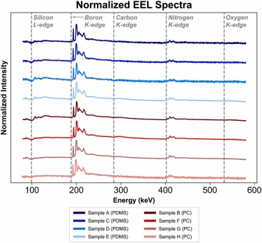
Bhatia, Pia; Shin, Trey T.; Kavetsky, Kyril; Sailors, Benjamin N.; Siokos, George; Uy-Tioco, Alexandra Sofia; Keneipp, Rachael N.; Gusdorff, Jordan A.; Bassett, Lee C.; Drndić, Marija
In: Micron, vol. 189, pp. 103747, 2024.
@article{Bhatia2024,

title = {A tale of two transfers: characterizing polydimethylsiloxane viscoelastic stamping and heated poly bis-A carbonate transfer of hexagonal boron nitride},

author = {Pia Bhatia and Trey T. Shin and Kyril Kavetsky and Benjamin N. Sailors and George Siokos and Alexandra Sofia Uy-Tioco and Rachael N. Keneipp and Jordan A. Gusdorff and Lee C. Bassett and Marija Drndić},

url = {https://www.sciencedirect.com/science/article/pii/S0968432824001641#sec0080},

doi = {10.1016/j.micron.2024.103747},

year  = {2024},

date = {2024-11-26},

urldate = {2024-11-26},

journal = {Micron},

volume = {189},

pages = {103747},

abstract = {Two-dimensional (2D) materials have many applications ranging from heterostructure electronics to nanofluidics and quantum technology. In order to effectively utilize 2D materials towards these ends, they must be transferred and integrated into complex device geometries. In this report, we investigate two conventional methods for the transfer of 2D materials: viscoelastic stamping with polydimethylsiloxane (PDMS) and a heated transfer with poly bis-A carbonate (PC). We use both methods to transfer mechanically-exfoliated flakes of hexagonal boron nitride onto silicon nitride (SiNx) substrates and characterize the resulting transfers using atomic force microscopy (AFM), aberration-corrected scanning transmission electron microscopy (AC-STEM) and electron energy loss spectroscopy (EELS). We find that both transfer methods yield flakes with significant and comparable residue (within the limitations of our study on eight samples). Qualitative interpretation of EELS maps demonstrates that this residue is comprised of silicon, carbon and oxygen for both transfer methods. Quantitative analysis of AC-STEM images reveals that the area covered in residue is on average, slightly lower for PDMS transfers (31 % ± 1 %), compared to PC transfers (41 % ± 4 %). This work underscores the importance of improving existing transfer protocols towards applications where cleaner materials are critical, as well as the need for robust methods to clean 2D materials.},

keywords = {},

pubstate = {published},

tppubtype = {article}

}
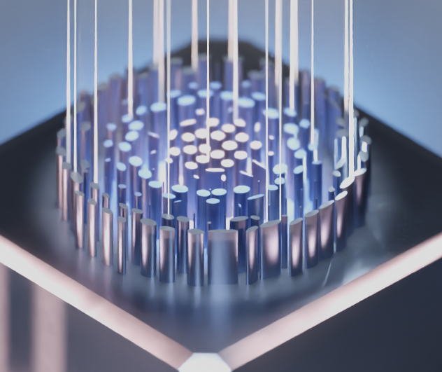
Klein, Amelia R.; Engheta, Nader; Bassett, Lee C.
Designing metasurface optical interfaces for solid-state qubits using many-body adjoint shape optimization Journal Article
In: Optics Express, vol. 32, iss. 22, pp. 38504-38515, 2024.
@article{Klein2024,

title = {Designing metasurface optical interfaces for solid-state qubits using many-body adjoint shape optimization},

author = {Amelia R. Klein and Nader Engheta and Lee C. Bassett},

url = {https://opg.optica.org/oe/fulltext.cfm?uri=oe-32-22-38504&id=561330

https://arxiv.org/abs/2406.08212},

doi = {10.1364/OE.522501},

year  = {2024},

date = {2024-10-09},

urldate = {2024-10-09},

journal = {Optics Express},

volume = {32},

issue = {22},

pages = {38504-38515},

abstract = {We present a general strategy for the inverse design of metasurfaces composed of elementary shapes. We use it to design a structure that collects and collimates light from nitrogen-vacancy centers in diamond. Such metasurfaces constitute scalable optical interfaces for solid-state qubits, enabling efficient photon coupling into optical fibers and eliminating free-space collection optics. The many-body shape optimization strategy is a practical alternative to topology optimization that explicitly enforces material and fabrication constraints throughout the optimization, while still achieving high performance. The metasurface is easily adaptable to other solid-state qubits, and the optimization method is broadly applicable to fabrication-constrained photonic design problems.},

keywords = {},

pubstate = {published},

tppubtype = {article}

}
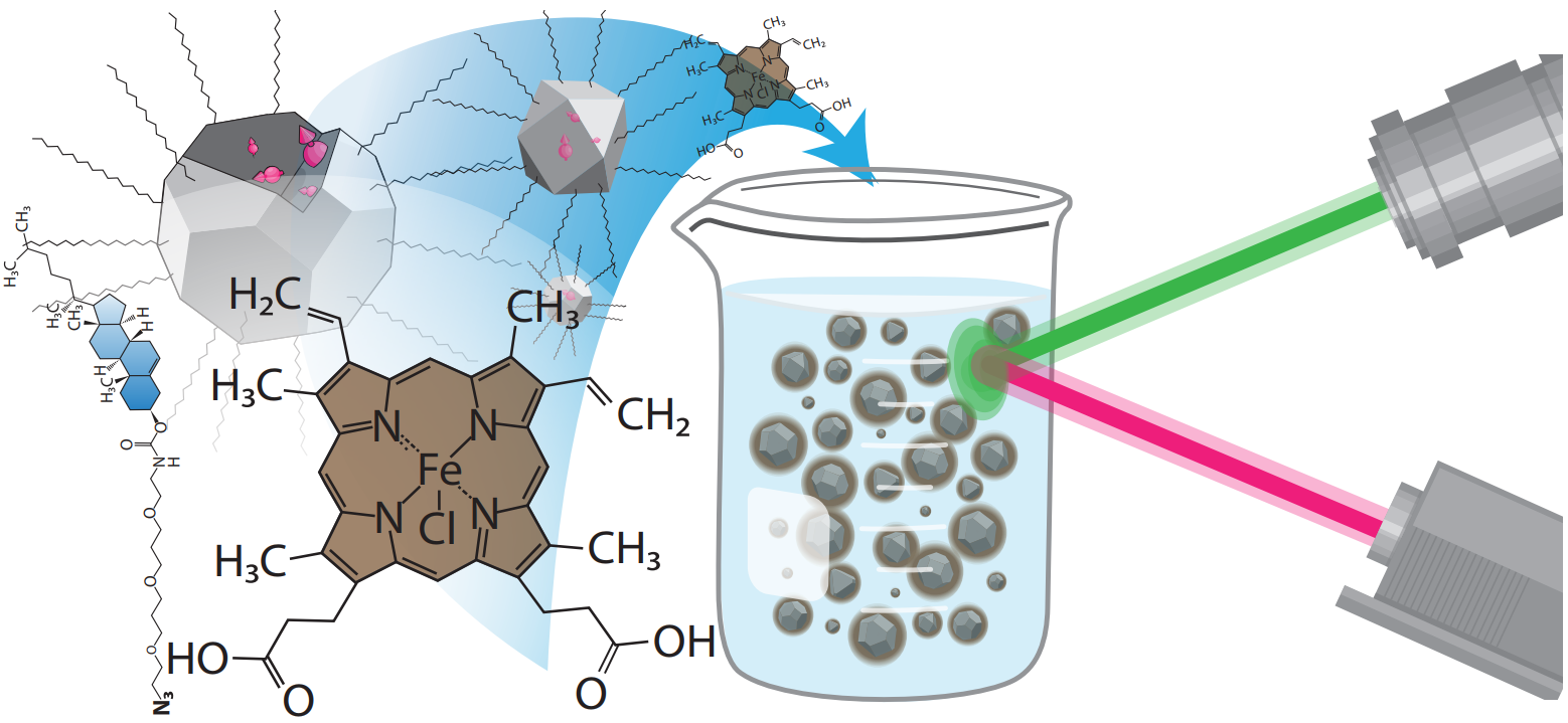
Shulevitz, Henry J.; Amirshaghaghi, Ahmad; Ouellet, Mathieu; Brustoloni, Caroline; Yang, Shengsong; Ng, Jonah J.; Huang, Tzu-Yung; Jishkariani, Davit; Murray, Christopher B.; Tsourkas, Andrew; Kagan, Cherie R.; Bassett, Lee C.
Nanodiamond emulsions for enhanced quantum sensing and click-chemistry conjugation Journal Article
In: ACS Applied Nano Materials, vol. 7, iss. 13, pp. 15334-15343, 2024.
@article{Shulevitz2024,

title = {Nanodiamond emulsions for enhanced quantum sensing and click-chemistry conjugation},

author = {Henry J. Shulevitz and Ahmad Amirshaghaghi and Mathieu Ouellet and Caroline Brustoloni and Shengsong Yang and Jonah J. Ng and Tzu-Yung Huang and Davit Jishkariani and Christopher B. Murray and Andrew Tsourkas and Cherie R. Kagan and Lee C. Bassett},

url = {https://pubs.acs.org/doi/abs/10.1021/acsanm.4c01699

https://arxiv.org/abs/2311.16530},

doi = {10.1021/acsanm.4c01699},

year  = {2024},

date = {2024-06-29},

urldate = {2024-06-29},

journal = {ACS Applied Nano Materials},

volume = {7},

issue = {13},

pages = {15334-15343},

abstract = {Nanodiamonds containing nitrogen-vacancy (NV) centers can serve as colloidal quantum sensors of local fields in biological and chemical environments. However, nanodiamond surfaces are challenging to modify without degrading their colloidal stability or the NV center’s optical and spin properties. We present a simple and general method to coat nanodiamonds with a thin emulsion layer that preserves their quantum features, maintains their colloidal stability, and provides functional groups for subsequent cross-linking and click-chemistry conjugation reactions. To demonstrate this technique, we decorated nanodiamonds with combinations of carboxyl- and azide-terminated amphiphiles that enable conjugation using two different strategies. A theoretical model is developed to understand the effect of the emulsion layer on the NV center’s spin lifetime, and T1 relaxometry is employed to quantify the nanodiamonds’ chemical sensitivity to paramagnetic ions. This general approach to nanodiamond surface functionalization will enable advances in quantum nanomedicine and biological sensing.},

keywords = {},

pubstate = {published},

tppubtype = {article}

}
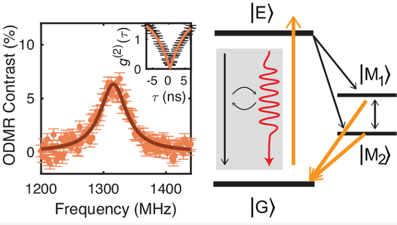
Patel, Raj N.; Fishman, Rebecca E. K.; Huang, Tzu-Yung; Gusdorff, Jordan A.; Fehr, David A.; Hopper, David A.; Breitweiser, S. Alex; Porat, Benjamin; Flatté, Michael E.; Bassett, Lee C.
Room Temperature Dynamics of an Optically Addressable Single Spin in Hexagonal Boron Nitride Journal Article
In: Nano Letters, vol. 24, iss. 25, pp. 7623-7628, 2024.
@article{Patel2024,

title = {Room Temperature Dynamics of an Optically Addressable Single Spin in Hexagonal Boron Nitride},

author = {Raj N. Patel and Rebecca E. K. Fishman and Tzu-Yung Huang and Jordan A. Gusdorff and David A. Fehr and David A. Hopper and S. Alex Breitweiser and Benjamin Porat and Michael E. Flatté and Lee C. Bassett},

url = {https://pubs.acs.org/doi/abs/10.1021/acs.nanolett.4c01333

https://arxiv.org/abs/2309.05604},

doi = {10.1021/acs.nanolett.4c01333},

year  = {2024},

date = {2024-06-11},

urldate = {2024-06-11},

journal = {Nano Letters},

volume = {24},

issue = {25},

pages = {7623-7628},

abstract = {Hexagonal boron nitride (h-BN) hosts pure single-photon emitters that have shown evidence of optically detected electronic spin dynamics. However, the electrical and chemical structures of these optically addressable spins are unknown, and the nature of their spin-optical interactions remains mysterious. Here, we use time-domain optical and microwave experiments to characterize a single emitter in h-BN exhibiting room temperature optically detected magnetic resonance. Using dynamical simulations, we constrain and quantify transition rates in the model, and we design optical control protocols that optimize the signal-to-noise ratio for spin readout. This constitutes a necessary step toward quantum control of spin states in h-BN.},

keywords = {},

pubstate = {published},

tppubtype = {article}

}
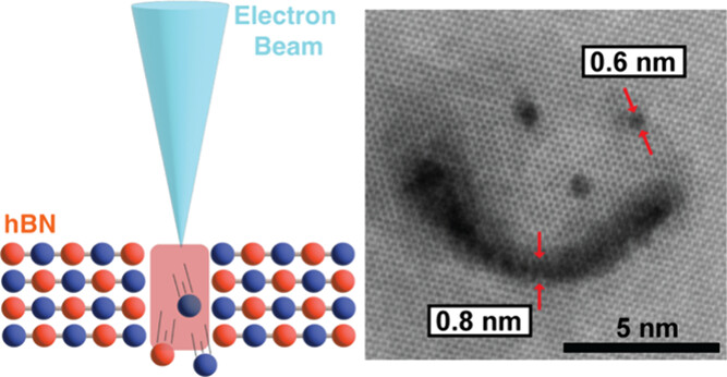
Keneipp, Rachael N.; Gusdorff, Jordan A.; Bhatia, Pia; Shin, Trey T.; Bassett, Lee C.; Drndić, Marija
Nanoscale Sculpting of Hexagonal Boron Nitride with an Electron Beam Journal Article
In: Journal of Physical Chemistry C, vol. 128, no. 21, pp. 8741–8749, 2024.
@article{Keneipp2024,

title = {Nanoscale Sculpting of Hexagonal Boron Nitride with an Electron Beam},

author = {Rachael N. Keneipp and Jordan A. Gusdorff and Pia Bhatia and Trey T. Shin and Lee C. Bassett and Marija Drndić},

url = {https://pubs.acs.org/doi/full/10.1021/acs.jpcc.4c02038},

doi = {10.1021/acs.jpcc.4c02038},

year  = {2024},

date = {2024-05-17},

journal = {Journal of Physical Chemistry C},

volume = {128},

number = {21},

pages = {8741–8749},

abstract = {Creating sub- to few-nanometer defects and nanopores in hexagonal boron nitride (hBN) opens opportunities for engineering quantum emitters and for nanofluidic and sensing applications. Using the electron beam in the aberration-corrected scanning transmission electron microscope, we demonstrate modification, thinning, and drilling of features in few-layer hBN membranes (∼5 to 20 nm-thick). The atomic composition is monitored with electron energy loss spectroscopy, which also facilitates drift correction. We report effects of electron beam energy and exposure times on defect size and structure. While previous studies focused on beam energies of ≤80 keV to avoid material damage, we show that drilling is favorable at a higher beam energy of 200 keV. The drilling rate at 200 keV is about 10 times larger than at 80 keV (∼1.2 vs 0.1 nm/min), and smaller pores are achievable with minimized damage to the surrounding material. Thinned hBN nanoscale features demonstrate enhanced emission via photoluminescence spectroscopy.},

keywords = {},

pubstate = {published},

tppubtype = {article}

}
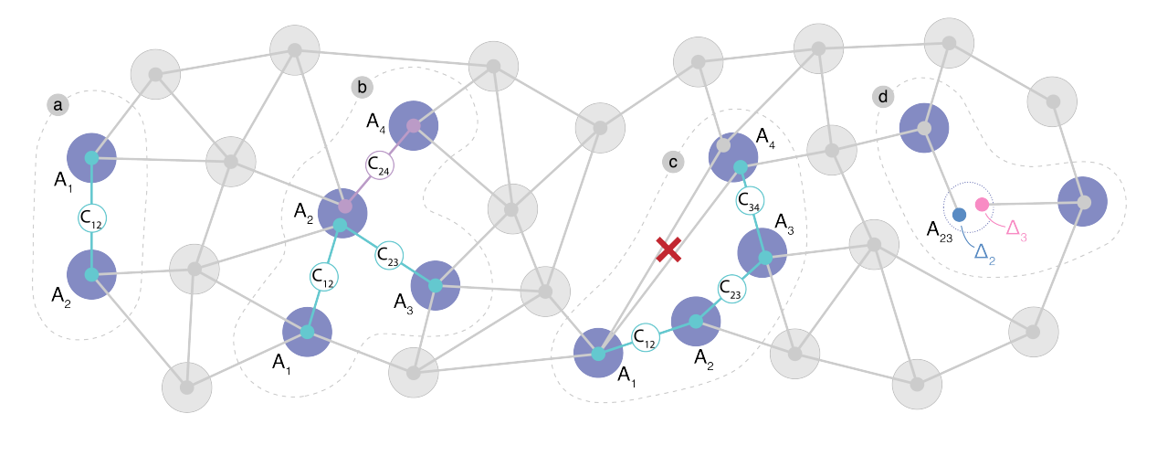
van de Stolpe, G. L.; Kwiatkowski, D. P.; Bradley, C. E.; Randall, J.; Breitweiser, S. A.; Bassett, L. C.; Markham, M.; Twitchen, D. J.; Taminiau, T. H.
Mapping a 50-spin-qubit network through correlated sensing Journal Article
In: Nature Communications , vol. 15, no. 2006, 2024.
@article{vandeStolpe2023,

title = {Mapping a 50-spin-qubit network through correlated sensing},

author = {G.L. van de Stolpe and D. P. Kwiatkowski and C.E. Bradley and J. Randall and S. A. Breitweiser and L. C. Bassett and M. Markham and D.J. Twitchen and T.H. Taminiau},

url = {https://arxiv.org/abs/2307.06939

https://www.nature.com/articles/s41467-024-46075-4},

doi = {10.1038/s41467-024-46075-4},

year  = {2024},

date = {2024-03-05},

journal = {Nature Communications },

volume = {15},

number = {2006},

abstract = {Spins associated to optically accessible solid-state defects have emerged as a versatile platform for exploring quantum simulation, quantum sensing and quantum communication. Pioneering experiments have shown the sensing, imaging, and control of multiple nuclear spins surrounding a single electron-spin defect. However, the accessible size and complexity of these spin networks has been constrained by the spectral resolution of current methods. Here, we map a network of 50 coupled spins through high-resolution correlated sensing schemes, using a single nitrogen-vacancy center in diamond. We develop concatenated double-resonance sequences that identify spin-chains through the network. These chains reveal the characteristic spin frequencies and their interconnections with high spectral resolution, and can be fused together to map out the network. Our results provide new opportunities for quantum simulations by increasing the number of available spin qubits. Additionally, our methods might find applications in nano-scale imaging of complex spin systems external to the host crystal.},

keywords = {},

pubstate = {published},

tppubtype = {article}

}

Gali, Adam; Schleife, André; Heinrich, Andreas J.; Laucht, Arne; Schuler, Bruno; Chakraborty, Chitraleema; Anderson, Christopher P.; Déprez, Corentin; McCallum, Jeffrey; Bassett, Lee C.; Friesen, Mark; Flatté, Michael E.; Maurer, Peter; Coppersmith, Susan N.; Zhong, Tian; Begum-Hudde, Vijaya; Ping, Yuan
Challenges in advancing our understanding of atomic-like quantum systems: Theory and experiment Journal Article
In: MRS Bulletin, vol. 49, pp. 256-276, 2024.
@article{Gali2024,

title = {Challenges in advancing our understanding of atomic-like quantum systems: Theory and experiment},

author = {Adam Gali and André Schleife and Andreas J. Heinrich and Arne Laucht and Bruno Schuler and Chitraleema Chakraborty and Christopher P. Anderson and Corentin Déprez and Jeffrey McCallum and Lee C. Bassett and Mark Friesen and Michael E. Flatté and Peter Maurer and Susan N. Coppersmith and Tian Zhong and Vijaya Begum-Hudde and Yuan Ping },

url = {https://link.springer.com/article/10.1557/s43577-023-00659-5},

doi = {10.1557/s43577-023-00659-5},

year  = {2024},

date = {2024-02-14},

journal = {MRS Bulletin},

volume = {49},

pages = {256-276},

abstract = {Quantum information processing and quantum sensing is a central topic for researchers who are part of the Materials Research Society and the Quantum Staging Group is providing leadership and guidance in this context. We convened a workshop before the 2022 MRS Spring Meeting and covered four topics to explore challenges that need to be addressed to further promote and accelerate the development of materials with applications in quantum technologies. This article captures the discussions at this workshop and refers to the pertinent literature.},

keywords = {},

pubstate = {published},

tppubtype = {article}

}
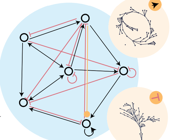
Ouellet, Mathieu; Kim, Jason Z; Guillaume, Harmange; Shaffer, Sydney M; Bassett, Lee C; Bassett, Dani S
Breaking reflection symmetry: evolving long dynamical cycles in Boolean systems Journal Article
In: New Journal of Physics, vol. 26, pp. 023006, 2024.
@article{Ouellet2024b,

title = {Breaking reflection symmetry: evolving long dynamical cycles in Boolean systems},

author = {Mathieu Ouellet and Jason Z Kim and Harmange Guillaume and Sydney M Shaffer and Lee C Bassett and Dani S Bassett},

url = {https://iopscience.iop.org/article/10.1088/1367-2630/ad1bdd/meta},

doi = {10.1088/1367-2630/ad1bdd},

year  = {2024},

date = {2024-02-06},

journal = {New Journal of Physics},

volume = {26},

pages = {023006},

abstract = {In interacting dynamical systems, specific local interaction rules for system components give rise to diverse and complex global dynamics. Long dynamical cycles are a key feature of many natural interacting systems, especially in biology. Examples of dynamical cycles range from circadian rhythms regulating sleep to cell cycles regulating reproductive behavior. Despite the crucial role of cycles in nature, the properties of network structure that give rise to cycles still need to be better understood. Here, we use a Boolean interaction network model to study the relationships between network structure and cyclic dynamics. We identify particular structural motifs that support cycles, and other motifs that suppress them. More generally, we show that the presence of dynamical reflection symmetry in the interaction network enhances cyclic behavior. In simulating an artificial evolutionary process, we find that motifs that break reflection symmetry are discarded. We further show that dynamical reflection symmetries are over-represented in Boolean models of natural biological systems. Altogether, our results demonstrate a link between symmetry and functionality for interacting dynamical systems, and they provide evidence for symmetry's causal role in evolving dynamical functionality.},

keywords = {},

pubstate = {published},

tppubtype = {article}

}
2023
Poteshman, Abigail N.; Ouellet, Mathieu; Bassett, Lee C.; Bassett, Dani S.
Network structure and dynamics of effective models of nonequilibrium quantum transport Journal Article
In: Physical Review Research, vol. 5, pp. 023125, 2023.
@article{Poteshman2023,

title = {Network structure and dynamics of effective models of nonequilibrium quantum transport},

author = {Abigail N. Poteshman and Mathieu Ouellet and Lee C. Bassett and Dani S. Bassett},

url = {https://journals.aps.org/prresearch/abstract/10.1103/PhysRevResearch.5.023125},

doi = {10.1103/PhysRevResearch.5.023125},

year  = {2023},

date = {2023-05-26},

journal = {Physical Review Research},

volume = {5},

pages = {023125},

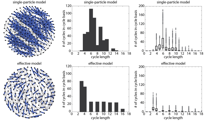
abstract = {Across all scales of the physical world, dynamical systems can be usefully represented as abstract networks that encode the systems' units and interunit interactions. Understanding how physical rules shape the topological structure of those networks can clarify a system's function and enhance our ability to design, guide, or control its behavior. In the emerging area of quantum network science, a key challenge lies in distinguishing between the topological properties that reflect a system's underlying physics and those that reflect the assumptions of the employed conceptual model. To elucidate and address this challenge, we study networks that represent nonequilibrium quantum-electronic transport through quantum antidot devices—an example of an open, mesoscopic quantum system. The network representations correspond to two different models of internal antidot states: a single-particle, noninteracting model and an effective model for collective excitations including Coulomb interactions. In these networks, nodes represent accessible energy states and edges represent allowed transitions. We find that both models reflect spin conservation rules in the network topology through bipartiteness and the presence of only even-length cycles. The models diverge, however, in the minimum length of cycle basis elements, in a manner that depends on whether electrons are considered to be distinguishable. Furthermore, the two models reflect spin-conserving relaxation effects differently, as evident in both the degree distribution and the cycle-basis length distribution. Collectively, these observations serve to elucidate the relationship between network structure and physical constraints in quantum-mechanical models. More generally, our approach underscores the utility of network science in understanding the dynamics of quantum systems.},

keywords = {},

pubstate = {published},

tppubtype = {article}

}
Omirzakhov, Kaisarbek; Idjadi, Mohamad Hossein; Huang, Tzu-Yung; Breitweiser, S. Alex; Hopper, David A.; Bassett, Lee C.; Aflatouni, Firooz
An Integrated Reconfigurable Spin Control System on 180 nm CMOS for Diamond NV Centers Journal Article
In: IEEE Transactions on Microwave Theory and Techniques, pp. 1-12, 2023.
@article{Omirzakhov2023,

title = {An Integrated Reconfigurable Spin Control System on 180 nm CMOS for Diamond NV Centers},

author = {Kaisarbek Omirzakhov and Mohamad Hossein Idjadi and Tzu-Yung Huang and S. Alex Breitweiser and David A. Hopper and Lee C. Bassett and Firooz Aflatouni},

url = {https://ieeexplore.ieee.org/document/10079193/keywords#keywords},

doi = {10.1109/TMTT.2023.3254600},

year  = {2023},

date = {2023-03-23},

journal = {IEEE Transactions on Microwave Theory and Techniques},

pages = {1-12},

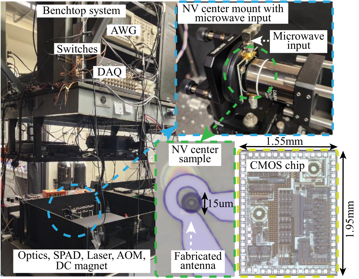
abstract = {Solid-state electron spins are key building blocks for emerging applications in quantum information science, including quantum computers, quantum communication links, and quantum sensors. These solid-state spins are mainly controlled using complex microwave pulse sequences, which are typically generated using benchtop electrical instruments. Integration of the required electronics will enable realization of a scalable low-power and compact optically addressable quantum system. Here, we report an integrated reconfigurable quantum control system, which is used to find electron-spin resonance (ESR) frequency and perform Rabi, Ramsey, and Hahn-echo measurements for a nitrogen-vacancy (NV) center spin qubit in diamond. The chip can be programmed to synthesize an RF signal tunable from 1.6 to 2.6 GHz, which is modulated with a sequence of up to 4098 reconfigurable pulses with a pulse width and pulse-to-pulse delay adjustable from 10 ns to 42 ms and 18 ns to 42 ms, respectively, at a resolution of 2.5 ns. The 180-nm CMOS chip is fabricated within a footprint of 3.02 mm 2 and has a power consumption of 80 mW.},

keywords = {},

pubstate = {published},

tppubtype = {article}

}
Thompson, Sarah M.; Şahin, Cüneyt; Yang, Shengsong; Flatté, Michael E.; Murray, Christopher B.; Bassett, Lee C.; Kagan, Cherie R.
Red Emission from Copper-Vacancy Color Centers in Zinc Sulfide Colloidal Nanocrystals Journal Article
In: ACS Nano, 2023.
@article{Thompson2023,

title = {Red Emission from Copper-Vacancy Color Centers in Zinc Sulfide Colloidal Nanocrystals},

author = {Sarah M. Thompson and Cüneyt Şahin and Shengsong Yang and Michael E. Flatté and Christopher B. Murray and Lee C. Bassett and Cherie R. Kagan},

url = {https://pubs.acs.org/doi/full/10.1021/acsnano.3c00191

https://arxiv.org/abs/2301.04223},

doi = {10.1021/acsnano.3c00191},

year  = {2023},

date = {2023-03-09},

journal = {ACS Nano},

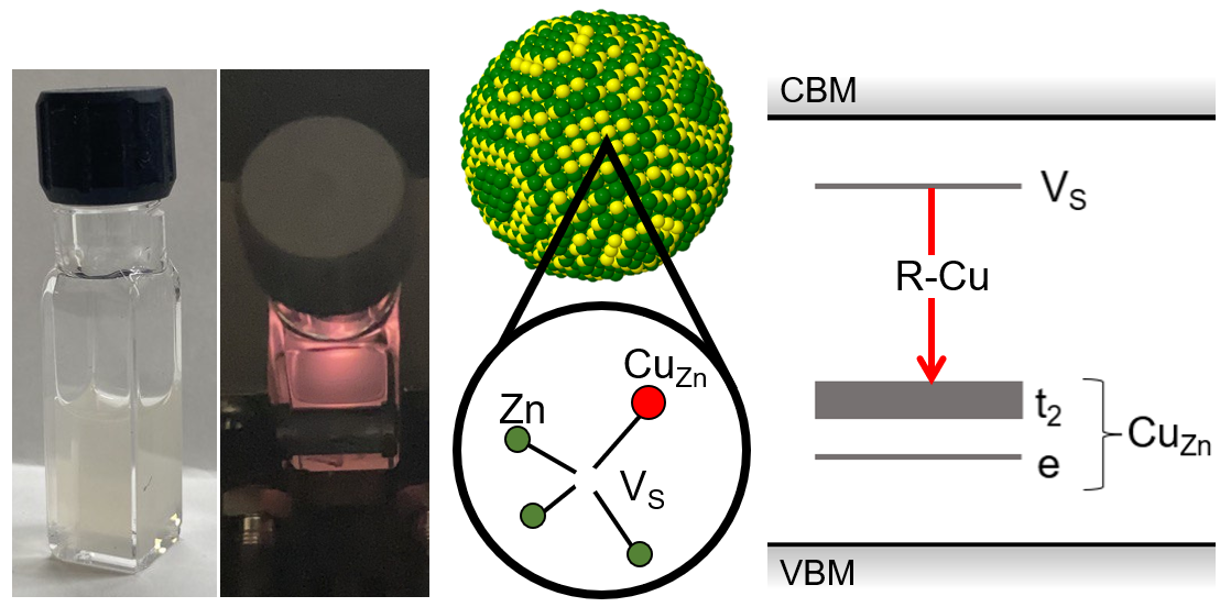
abstract = {Copper-doped zinc sulfide (ZnS:Cu) exhibits down-conversion luminescence in the UV, visible, and IR regions of the electromagnetic spectrum; the visible red, green, and blue emission is referred to as R-Cu, G-Cu, and B-Cu, respectively. The sub-bandgap emission arises from optical transitions between localized electronic states created by point defects, making ZnS:Cu a prolific phosphor material and an intriguing candidate material for quantum information science, where point defects excel as single-photon sources and spin qubits. Colloidal nanocrystals (NCs) of ZnS:Cu are particularly interesting as hosts for the creation, isolation, and measurement of quantum defects, since their size, composition, and surface chemistry can be precisely tailored for bio-sensing and opto-electronic applications. Here, we present a method for synthesizing colloidal ZnS:Cu NCs that emit primarily R-Cu, which has been proposed to arise from the CuZn-VS complex, an impurity-vacancy point defect structure analogous to well-known quantum defects in other materials that produce favorable optical and spin dynamics. First principles calculations confirm the thermodynamic stability and electronic structure of CuZn-VS. Temperature- and time-dependent optical properties of ZnS:Cu NCs show blueshifting luminescence and an anomalous plateau in the intensity dependence as temperature is increased from 19 K to 290 K, for which we propose an empirical dynamical model based on thermally-activated coupling between two manifolds of states inside the ZnS bandgap. Understanding of R-Cu emission dynamics, combined with a controlled synthesis method for obtaining R-Cu centers in colloidal NC hosts, will greatly facilitate the development of CuZn-VS and related complexes as quantum point defects in ZnS.},

keywords = {},

pubstate = {published},

tppubtype = {article}

}
Fishman, Rebecca E. K.; Patel, Raj N.; Hopper, David A.; Huang, Tzu-Yung; Bassett, Lee C.
Photon emission correlation spectroscopy as an analytical tool for quantum defects Journal Article
In: PRX Quantum, vol. 4, pp. 010202, 2023.
@article{Fishman2021,

title = {Photon emission correlation spectroscopy as an analytical tool for quantum defects},

author = {Rebecca E. K. Fishman and Raj N. Patel and David A. Hopper and Tzu-Yung Huang and Lee C. Bassett},

url = {https://journals.aps.org/prxquantum/abstract/10.1103/PRXQuantum.4.010202

https://arxiv.org/abs/2111.01252},

doi = {10.1103/PRXQuantum.4.010202},

year  = {2023},

date = {2023-03-06},

journal = {PRX Quantum},

volume = {4},

pages = {010202},

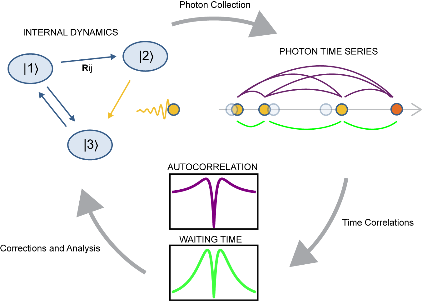
abstract = {Photon emission correlation spectroscopy has a long history in the study of atoms, molecules, and, more recently, solid-state quantum defects. In solid-state systems, its most common use is as an indicator of single-photon emission, a key property for quantum technology. However, photon correlation data can provide a wealth of information about quantum emitters beyond their single-photon purity−information that can reveal details about an emitter's electronic structure and optical dynamics that are hidden by other spectroscopy techniques. We present a standardized framework for using photon emission correlation spectroscopy to study quantum emitters, including discussion of theory, data acquisition, analysis, and interpretation. We highlight nuances and best practices regarding the commonly used g(2)(τ=0)<0.5 test for single-photon emission. Finally, we illustrate how this experimental technique can be paired with optical dynamics simulations to formulate an electronic model for unknown quantum emitters, enabling the design of quantum control protocols and assessment of their suitability for quantum information science applications.},

keywords = {},

pubstate = {published},

tppubtype = {article}

}
2022
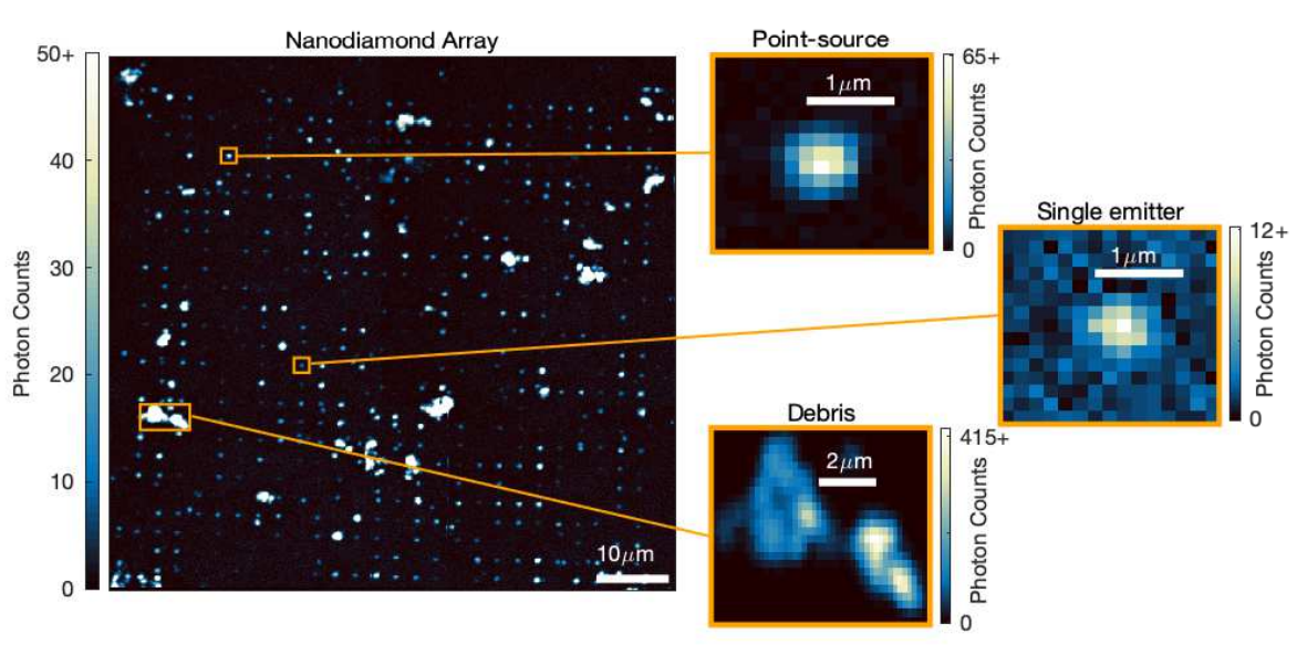
Narun, Leah R.; Fishman, Rebecca E. K.; Shulevitz, Henry J.; Patel, Raj N.; Bassett, Lee C.
Efficient Analysis of Photoluminescence Images for the Classification of Single-Photon Emitters Journal Article
In: ACS Photonics, vol. 9, no. 11, pp. 3540–3549, 2022.
@article{Narun2021,

title = {Efficient Analysis of Photoluminescence Images for the Classification of Single-Photon Emitters},

author = {Leah R. Narun and Rebecca E. K. Fishman and Henry J. Shulevitz and Raj N. Patel and Lee C. Bassett},

url = {https://pubs.acs.org/doi/10.1021/acsphotonics.2c00795

https://arxiv.org/abs/2112.05654},

doi = {10.1021/acsphotonics.2c00795},

year  = {2022},

date = {2022-10-31},

journal = {ACS Photonics},

volume = {9},

number = {11},

pages = {3540–3549},

abstract = {Solid-state single-photon emitters (SPE) are a basis for emerging technologies such as quantum communication and quantum sensing. SPE based on fluorescent point defects are ubiquitous in semiconductors and insulators, and new systems with desirable properties for quantum information science may exist amongst the vast number of unexplored defects. However, the characterization of new SPE typically relies on time-consuming techniques for identifying point source emitters by eye in photoluminescence (PL) images. This manual strategy is a bottleneck for discovering new SPE, motivating a more efficient method for characterizing emitters in PL images. Here we present a quantitative method using image analysis and regression fitting to automatically identify Gaussian emitters in PL images and classify them according to their stability, shape, and intensity relative to the background. We demonstrate efficient emitter classification for SPEs in nanodiamond arrays and hexagonal boron nitride flakes. Adaptive criteria detect SPE in both samples despite variation in emitter intensity, stability, and background features. The detection criteria can be tuned for specific material systems and experimental setups to accommodate the diverse properties of SPE.},

keywords = {},

pubstate = {published},

tppubtype = {article}

}
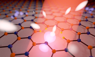
Patel, Raj N.; Hopper, David A.; Gusdorff, Jordan A.; Turiansky, Mark E.; Huang, Tzu-Yung; Fishman, Rebecca E. K.; Porat, Benjamin; de Walle, Chris G. Van; Bassett, Lee C.
Probing the Optical Dynamics of Quantum Emitters in Hexagonal Boron Nitride Journal Article
In: PRX Quantum, vol. 3, no. 3, pp. 030331, 2022.
@article{Patel2022,

title = {Probing the Optical Dynamics of Quantum Emitters in Hexagonal Boron Nitride},

author = {Raj N. Patel and David A. Hopper and Jordan A. Gusdorff and Mark E. Turiansky and Tzu-Yung Huang and Rebecca E. K. Fishman and Benjamin Porat and Chris G. Van de Walle and Lee C. Bassett},

url = {https://journals.aps.org/prxquantum/abstract/10.1103/PRXQuantum.3.030331},

doi = {10.1103/PRXQuantum.3.030331},

year  = {2022},

date = {2022-09-01},

journal = {PRX Quantum},

volume = {3},

number = {3},

pages = {030331},

abstract = {Hexagonal boron nitride is a van der Waals material that hosts visible-wavelength quantum emitters at room temperature. However, experimental identification of the quantum emitters’ electronic structure is lacking, and key details of their charge and spin properties remain unknown. Here, we probe the optical dynamics of quantum emitters in hexagonal boron nitride using photon emission correlation spectroscopy. Several quantum emitters exhibit ideal single-photon emission with noise-limited photon antibunching, g(2)(0)=0. The photoluminescence emission lineshapes are consistent with individual vibronic transitions. However, polarization-resolved excitation and emission suggests the role of multiple optical transitions, and photon emission correlation spectroscopy reveals complicated optical dynamics associated with excitation and relaxation through multiple electronic excited states. We compare the experimental results to quantitative optical dynamics simulations, develop electronic structure models that are consistent with the observations, and discuss the results in the context of ab initio theoretical calculations.},

keywords = {},

pubstate = {published},

tppubtype = {article}

}
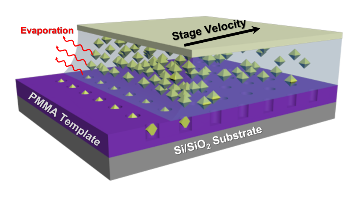
Shulevitz, Henry J.; Huang, Tzu-Yung; Xu, Jun; Neuhaus, Steven; Patel, Raj N.; Lee C. Bassett, Cherie R. Kagan
Template-Assisted Self Assembly of Fluorescent Nanodiamonds for Scalable Quantum Technologies Journal Article
In: ACS Nano, vol. 16, no. 2, pp. 1847–1856, 2022.
@article{Shulevitz2021,

title = {Template-Assisted Self Assembly of Fluorescent Nanodiamonds for Scalable Quantum Technologies},

author = {Henry J. Shulevitz and Tzu-Yung Huang and Jun Xu and Steven Neuhaus and Raj N. Patel and Lee C. Bassett, Cherie R. Kagan},

url = {https://arxiv.org/abs/2111.14921},

doi = {10.1021/acsnano.1c09839},

year  = {2022},

date = {2022-01-13},

journal = {ACS Nano},

volume = {16},

number = {2},

pages = {1847–1856},

abstract = {Milled nanodiamonds containing nitrogen-vacancy (NV) centers provide an excellent platform for sensing applications as they are optically robust, have nanoscale quantum sensitivity, and form colloidal dispersions which enable bottom-up assembly techniques for device integration. However, variations in their size, shape, and surface chemistry limit the ability to position individual nanodiamonds and statistically study properties that affect their optical and quantum characteristics. Here, we present a scalable strategy to form ordered arrays of nanodiamonds using capillary-driven, template-assisted self assembly. This method enables the precise spatial arrangement of isolated nanodiamonds with diameters below 50 nm across millimeter-scale areas. Measurements of over 200 assembled nanodiamonds yield a statistical understanding of their structural, optical, and quantum properties. The NV centers' spin and charge properties are uncorrelated with nanodiamond size, but rather are consistent with heterogeneity in their nanoscale environment. This flexible assembly method, together with improved understanding of the material, will enable the integration of nanodiamonds into future quantum photonic and electronic devices.},

keywords = {},

pubstate = {published},

tppubtype = {article}

}
2020
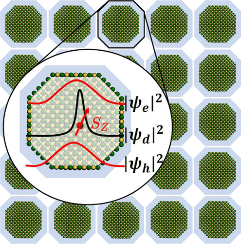
Kagan, Cherie R.; Bassett, Lee C.; Murray, Christopher B.; Thompson, Sarah M.
Colloidal Quantum Dots as Platforms for Quantum Information Science Journal Article
In: Chemical Reviews, 2020.
@article{Kagan2020,

title = {Colloidal Quantum Dots as Platforms for Quantum Information Science},

author = {Cherie R. Kagan and Lee C. Bassett and Christopher B. Murray and Sarah M. Thompson},

url = {https://pubs.acs.org/doi/10.1021/acs.chemrev.0c00831},

doi = {10.1021/acs.chemrev.0c00831},

year  = {2020},

date = {2020-12-29},

journal = {Chemical Reviews},

abstract = {Colloidal quantum dots (QDs) are nanoscale semiconductor crystals with surface ligands that enable their dispersion in solvents. Quantum confinement effects facilitate wave function engineering to sculpt the spatial distribution of charge and spin states and thus the energy and dynamics of QD optical transitions. Colloidal QDs can be integrated in devices using solution-based assembly methods to position single QDs and to create ordered QD arrays. Here, we describe the synthesis, assembly, and photophysical properties of colloidal QDs that have captured scientific imagination and have been harnessed in optical applications. We focus especially on the current understanding of their quantum coherent effects and opportunities to exploit QDs as platforms for quantum information science. Freedom in QD design to isolate and control the quantum mechanical properties of charge, spin, and light presents various approaches to create systems with robust, addressable quantum states. We consider the attributes of QDs for optically addressable qubits in emerging quantum computation, sensing, simulation, and communication technologies, e.g., as robust sources of indistinguishable, single photons that can be integrated into photonic structures to amplify, direct, and tune their emission or as hosts for isolated, coherent spin states that can be coupled to light or to other spins in QD arrays.},

keywords = {},

pubstate = {published},

tppubtype = {article}

}
Bassett, L C
Quantum optics with single spins Book Chapter
In: Irene D’Amico Mario Agio, Rashid Zia (Ed.): vol. 204, pp. 115-144, IOS Press, 2020, ISBN: 978-1-64368-099-6.
@inbook{Bassett2019,

title = {Quantum optics with single spins},

author = {L C Bassett},

editor = {Mario Agio, Irene D’Amico, Rashid Zia, Costanza Toninelli},

url = {https://ebooks.iospress.nl/doi/10.3254/ENFI200022

https://arxiv.org/abs/1908.05566},

doi = {10.3254/ENFI200022},

isbn = {978-1-64368-099-6},

year  = {2020},

date = {2020-12-16},

volume = {204},

pages = {115-144},

publisher = {IOS Press},

series = {Proceedings of the International School of Physics "Enrico Fermi"},

abstract = {Based on lectures at the 2018 International School of Physics "Enrico Fermi", Course 204: Nanoscale Quantum Optics


Defects in solids are in many ways analogous to trapped atoms or molecules. They can serve as long-lived quantum memories and efficient light-matter interfaces. As such, they are leading building blocks for long-distance quantum networks and distributed quantum computers. This chapter describes the quantum-mechanical coupling between atom-like spin states and light, using the diamond nitrogen-vacancy (NV) center as a paradigm. We present an overview of the NV center's electronic structure, derive a general picture of coherent light-matter interactions, and describe several methods that can be used to achieve all-optical initialization, quantum-coherent control, and readout of solid-state spins. These techniques can be readily generalized to other defect systems, and they serve as the basis for advanced protocols at the heart of many emerging quantum technologies.},

keywords = {},

pubstate = {published},

tppubtype = {inbook}

}
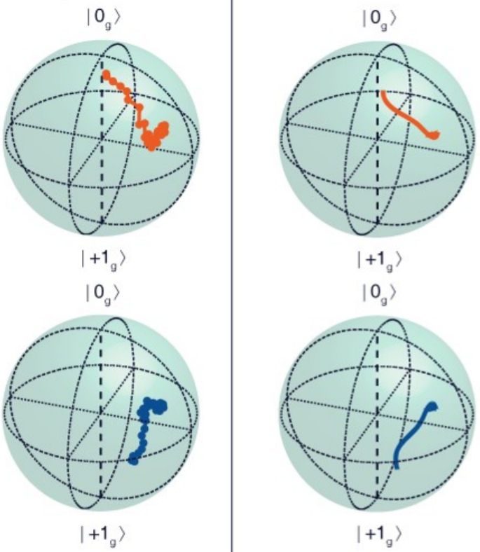
Defects in solids are in many ways analogous to trapped atoms or molecules. They can serve as long-lived quantum memories and efficient light-matter interfaces. As such, they are leading building blocks for long-distance quantum networks and distributed quantum computers. This chapter describes the quantum-mechanical coupling between atom-like spin states and light, using the diamond nitrogen-vacancy (NV) center as a paradigm. We present an overview of the NV center's electronic structure, derive a general picture of coherent light-matter interactions, and describe several methods that can be used to achieve all-optical initialization, quantum-coherent control, and readout of solid-state spins. These techniques can be readily generalized to other defect systems, and they serve as the basis for advanced protocols at the heart of many emerging quantum technologies.
Hopper, D A; Lauigan, J D; Huang, T -Y; Bassett, L C
Real-Time Charge Initialization of Diamond Nitrogen-Vacancy Centers for Enhanced Spin Readout Journal Article
In: Phys. Rev. Applied, vol. 13, pp. 024016, 2020.
@article{Hopper2019,

title = {Real-Time Charge Initialization of Diamond Nitrogen-Vacancy Centers for Enhanced Spin Readout},

author = {D A Hopper and J D Lauigan and T -Y Huang and L C Bassett},

url = {https://arxiv.org/abs/1907.08741

https://journals.aps.org/prapplied/abstract/10.1103/PhysRevApplied.13.024016

https://medium.com/penn-engineering/penn-engineers-ensure-quantum-experiments-get-off-to-the-right-start-bbe6f3382cb},

year  = {2020},

date = {2020-02-07},

journal = {Phys. Rev. Applied},

volume = {13},

pages = {024016},

abstract = {Selected as an Editor's Suggestion.


A common impediment to qubit performance is imperfect state initialization. In the case of the diamond nitrogen-vacancy (NV) center, the initialization fidelity is limited by fluctuations in the defect's charge state during optical pumping. Here, we use real-time control to deterministically initialize the NV center's charge state at room temperature. We demonstrate a maximum charge initialization fidelity of 99.4±0.1% and present a quantitative model of the initialization process that allows for systems-level optimization of the spin-readout signal-to-noise ratio. Even accounting for the overhead associated with the initialization sequence, increasing the charge initialization fidelity from the steady-state value of 75% near to unity allows for a factor-of-two speedup in experiments while maintaining the same signal-to-noise-ratio. In combination with high-fidelity readout based on spin-to-charge conversion, real-time initialization enables a factor-of-20 speedup over traditional methods, resulting in an ac magnetic sensitivity of 1.3 nT/Hz1/2 for our single NV-center spin. The real-time control method is immediately beneficial for quantum sensing applications with NV centers as well as probing charge-dependent physics, and it will facilitate protocols for quantum feedback control over multi-qubit systems.},

keywords = {},

pubstate = {published},

tppubtype = {article}

}
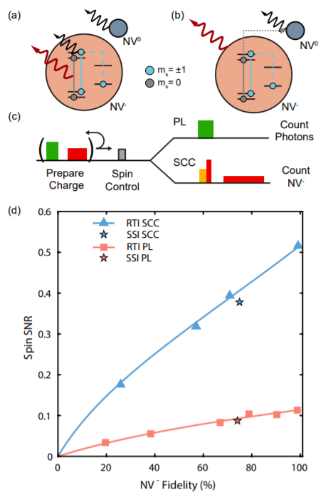
A common impediment to qubit performance is imperfect state initialization. In the case of the diamond nitrogen-vacancy (NV) center, the initialization fidelity is limited by fluctuations in the defect's charge state during optical pumping. Here, we use real-time control to deterministically initialize the NV center's charge state at room temperature. We demonstrate a maximum charge initialization fidelity of 99.4±0.1% and present a quantitative model of the initialization process that allows for systems-level optimization of the spin-readout signal-to-noise ratio. Even accounting for the overhead associated with the initialization sequence, increasing the charge initialization fidelity from the steady-state value of 75% near to unity allows for a factor-of-two speedup in experiments while maintaining the same signal-to-noise-ratio. In combination with high-fidelity readout based on spin-to-charge conversion, real-time initialization enables a factor-of-20 speedup over traditional methods, resulting in an ac magnetic sensitivity of 1.3 nT/Hz1/2 for our single NV-center spin. The real-time control method is immediately beneficial for quantum sensing applications with NV centers as well as probing charge-dependent physics, and it will facilitate protocols for quantum feedback control over multi-qubit systems.
2019
Poteshman, Abigail N; Tang, Evelyn; Papadopoulos, Lia; Bassett, Danielle S; Bassett, Lee C
Network architecture of energy landscapes in mesoscopic quantum systems Journal Article
In: New Journal of Physics, vol. 21, pp. 123049, 2019.
@article{Poteshman2019,

title = {Network architecture of energy landscapes in mesoscopic quantum systems},

author = {Abigail N Poteshman and Evelyn Tang and Lia Papadopoulos and Danielle S Bassett and Lee C Bassett},

url = {https://iopscience.iop.org/article/10.1088/1367-2630/ab5c9f

https://arxiv.org/abs/1811.12382},

doi = {10.1088/1367-2630/ab5c9f},

year  = {2019},

date = {2019-12-20},

journal = {New Journal of Physics},

volume = {21},

pages = {123049},

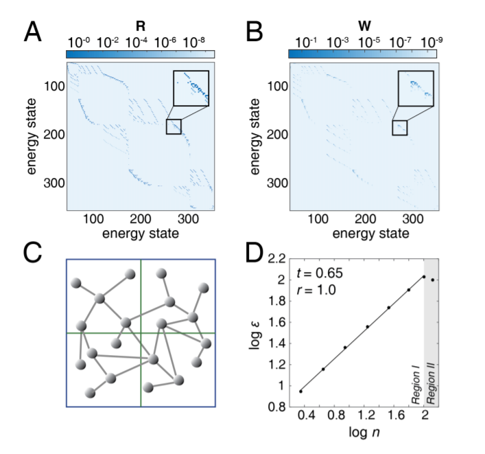
abstract = {Mesoscopic quantum systems exhibit complex many-body quantum phenomena, where interactions between spins and charges give rise to collective modes and topological states. Even simple, non-interacting theories display a rich landscape of energy states --- distinct many-particle configurations connected by spin- and energy-dependent transition rates. The collective energy landscape is difficult to characterize or predict, especially in regimes of frustration where many-body effects create a multiply degenerate landscape. Here we use network science to characterize the complex interconnection patterns of these energy-state transitions. Using an experimentally verified computational model of electronic transport through quantum antidots, we construct networks where nodes represent accessible energy states and edges represent allowed transitions. We then explore how physical changes in currents and voltages are reflected in the network topology. We find that the networks exhibit Rentian scaling, which is characteristic of efficient transportation systems in computer circuitry, neural circuitry, and human mobility, and can be used to measure the interconnection complexity of a network. Remarkably, networks corresponding to points of frustration in quantum transport (due, for example, to spin-blockade effects) exhibit an enhanced topological complexity relative to networks not experiencing frustration. Our results demonstrate that network characterizations of the abstract topological structure of energy landscapes can capture salient properties of quantum transport. More broadly, our approach motivates future efforts to use network science in understanding the dynamics and control of complex quantum systems.},

keywords = {},

pubstate = {published},

tppubtype = {article}

}
Breitweiser, S A; Exarhos, A L; Patel, R N; Saouaf, J; Porat, B; Hopper, D A; Bassett, L C
Efficient optical quantification of heterogeneous emitter ensembles Journal Article
In: ACS Photonics, vol. 7, pp. 288-295, 2019.
@article{Breitweiser2019,

title = {Efficient optical quantification of heterogeneous emitter ensembles},

author = {S A Breitweiser and A L Exarhos and R N Patel and J Saouaf and B Porat and D A Hopper and L C Bassett},

url = {https://arxiv.org/abs/1909.12726

https://pubs.acs.org/doi/10.1021/acsphotonics.9b01707},

year  = {2019},

date = {2019-12-17},

journal = {ACS Photonics},

volume = {7},

pages = {288-295},

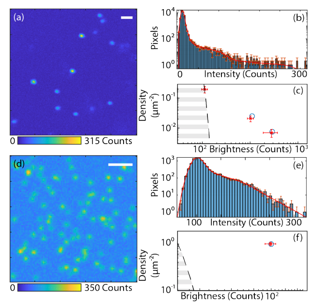
abstract = {Defect-based quantum emitters in solid state materials offer a promising platform for quantum communication and sensing. Confocal fluorescence microscopy techniques have revealed quantum emitters in a multitude of host materials. In some materials, however, optical properties vary widely between emitters, even within the same sample. In these cases, traditional ensemble fluorescence measurements are confounded by heterogeneity, whereas individual defect-by-defect studies are impractical. Here, we develop a method to quantitatively and systematically analyze the properties of heterogeneous emitter ensembles using large-area photoluminescence maps. We apply this method to study the effects of sample treatments on emitters in hexagonal boron nitride, and we find that low-energy (3 keV) electron irradiation creates emitters, whereas high-temperature (850 ∘C) annealing in an inert gas environment brightens emitters.},

keywords = {},

pubstate = {published},

tppubtype = {article}

}
Brown, K. J.; Chartier, E.; Sweet, E. M.; A.Hopper, D.; Bassett, L. C.
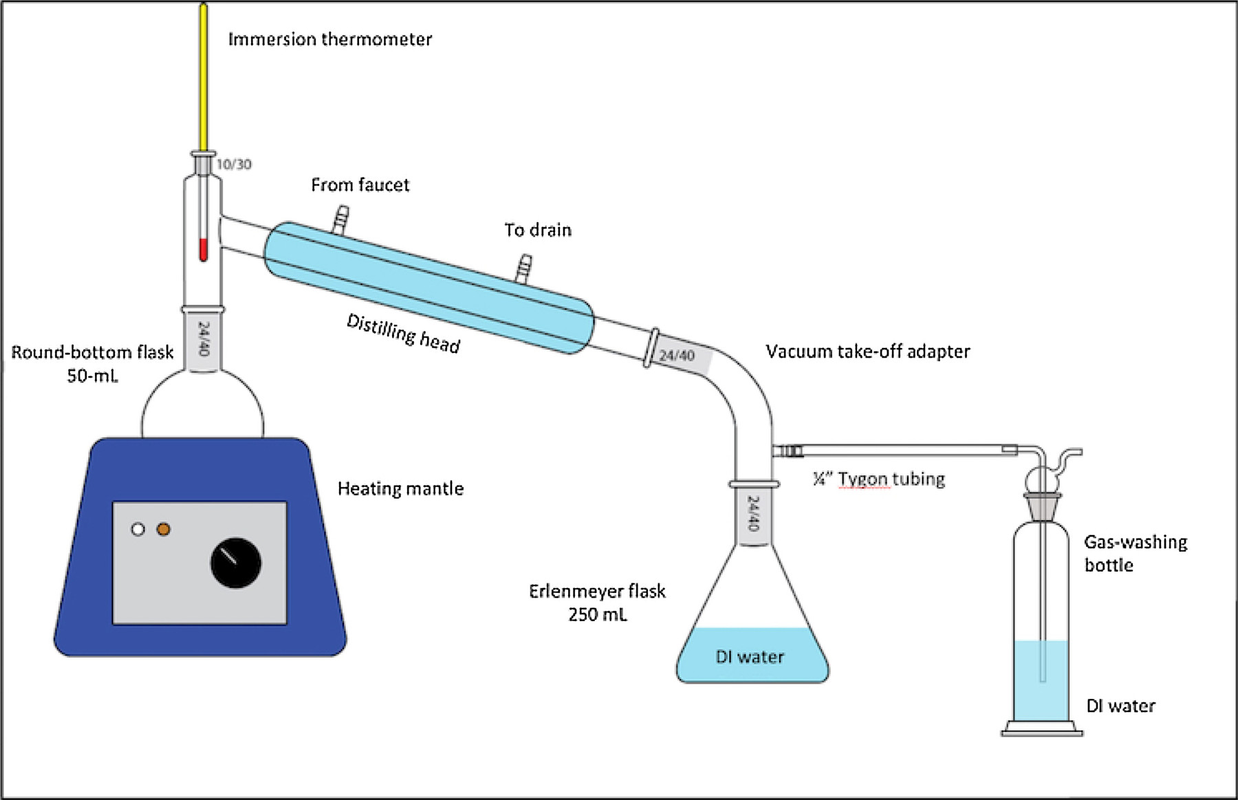
Cleaning diamond surfaces using boiling acid treatment in a standard laboratory chemical hood Journal Article
In: Journal of Chemical Health and Safety, vol. 26, pp. 40-44, 2019.
@article{Brown2019,

title = {Cleaning diamond surfaces using boiling acid treatment in a standard laboratory chemical hood},

author = {K. J. Brown and E. Chartier and E. M. Sweet and D. A.Hopper and L. C. Bassett},

url = {https://pubs.acs.org/doi/10.1021/acs.chas.8b26611},

year  = {2019},

date = {2019-11-01},

journal = {Journal of Chemical Health and Safety},

volume = {26},

pages = {40-44},

abstract = {Diamond is the basis for numerous applications in optics, electronics, and quantum science due to its desirable material properties and the existence of optically active spins such as the nitrogen-vacancy (NV) center. For some applications, pristine diamond surfaces are required. However, treatments such as irradiation and high-temperature annealing used to create NV centers produce unwanted graphitic and pyrolytic domains of carbon that are difficult to remove using most chemical treatments. A boiling mixture of nitric, perchloric, and sulfuric acids is known to selectively etch graphitic carbon and is commonly used in the research community to restore a clean diamond surface. The risks associated with using these acids, in the presence of organic material, are explosion due to the potential creation of perchlorate salts, as well as ignition due to the presence of an oxygen source from all three acids and a fuel source from the organic material. In this paper, we will discuss a method that mitigates these risks of the cleaning process without requiring a special laboratory chemical hood with a wash-down feature. This method was brought to the attention of health and safety staff after a research group at The University of Pennsylvania requested information about the safety of the procedure and preventative controls.},

keywords = {},

pubstate = {published},

tppubtype = {article}

}
Bassett, L. C.; Alkauskas, A.; Exarhos, A. L.; Fu, K. -M. C.
Quantum defects by design Journal Article
In: Nanophotonics, vol. 8, no. 11, 2019.
@article{Bassett2019b,

title = {Quantum defects by design},

author = {L. C. Bassett and A. Alkauskas and A. L. Exarhos and K.-M. C. Fu},

url = {https://www.degruyter.com/view/journals/nanoph/8/11/article-p1867.xml},

year  = {2019},

date = {2019-10-04},

journal = {Nanophotonics},

volume = {8},

number = {11},

abstract = {Part of Special Issue on Quantum Nanophotonics in Emerging Materials.


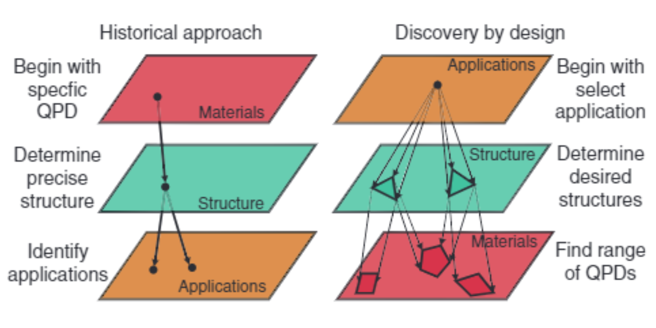
Miniaturization of electronic and opto-electronic semiconductor devices has been happening ever since the first such devices appeared. Eventually, one can envision a device that is composed of just a few atoms. As these atoms ideally should not float in free space, but should be embedded in a solid-state matrix, this naturally brings one to the concept of a point defect (an impurity atom or complex of atoms) as the ultimate electronic or opto-electronic device. At such tiny length scales the behavior of physical systems is governed by the laws of quantum mechanics. Therefore, it is no surprise that an increasing number of point defects are being considered as building blocks for various applications in the field of quantum information science; more specifically, in quantum sensing, quantum communication, and quantum computing [1], [2], [3], [4]. We refer to these desirable defects as quantum point defects (QPDs). Prominent examples include the nitrogen-vacancy (NV) center in diamond, the silicon-vacancy (SiV) center in diamond, the divacancy in silicon carbide, and rare-earth impurities in complex oxides.},

keywords = {},

pubstate = {published},

tppubtype = {article}

}
Miniaturization of electronic and opto-electronic semiconductor devices has been happening ever since the first such devices appeared. Eventually, one can envision a device that is composed of just a few atoms. As these atoms ideally should not float in free space, but should be embedded in a solid-state matrix, this naturally brings one to the concept of a point defect (an impurity atom or complex of atoms) as the ultimate electronic or opto-electronic device. At such tiny length scales the behavior of physical systems is governed by the laws of quantum mechanics. Therefore, it is no surprise that an increasing number of point defects are being considered as building blocks for various applications in the field of quantum information science; more specifically, in quantum sensing, quantum communication, and quantum computing [1], [2], [3], [4]. We refer to these desirable defects as quantum point defects (QPDs). Prominent examples include the nitrogen-vacancy (NV) center in diamond, the silicon-vacancy (SiV) center in diamond, the divacancy in silicon carbide, and rare-earth impurities in complex oxides.
Turiansky, M E; Alkauskas, A; Bassett, L C; de Walle, Van C G
Dangling bonds in hexagonal boron nitride as single-photon emitters Journal Article
In: Physical Review Letters, vol. 123, no. 12, pp. 127401, 2019, ISSN: 1079-7114.
@article{Turiansky2019,

title = {Dangling bonds in hexagonal boron nitride as single-photon emitters},

author = {M E Turiansky and A Alkauskas and L C Bassett and Van C G de Walle},

url = {https://journals.aps.org/prl/abstract/10.1103/PhysRevLett.123.127401},

doi = {10.1103},

issn = {1079-7114},

year  = {2019},

date = {2019-09-16},

journal = {Physical Review Letters},

volume = {123},

number = {12},

pages = {127401},

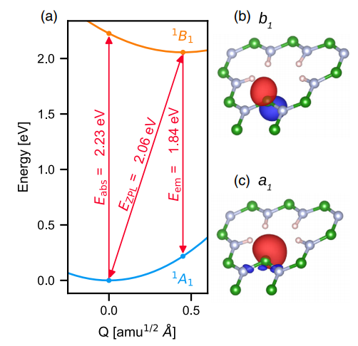
abstract = {Hexagonal boron nitride has been found to host color centers that exhibit single-photon emission, but the microscopic origin of these emitters is unknown. We propose boron dangling bonds as the likely source of the observed single-photon emission around 2 eV. An optical transition where an electron is excited from a doubly occupied boron dangling bond to a localized B pz state gives rise to a zero-phonon line of 2.06 eV and emission with a Huang-Rhys factor of 2.3. This transition is linearly polarized with the absorptive and emissive dipole aligned. Because of the energetic position of the states within the band gap, indirect excitation through the conduction band will occur for sufficiently large excitation energies, leading to the misalignment of the absorptive and emissive dipoles seen in experiment. Our calculations predict a singlet ground state and the existence of a metastable triplet state, in agreement with experiment.},

keywords = {},

pubstate = {published},

tppubtype = {article}

}
Huang, T -Y; Grote, R R; Mann, S A; Hopper, D A; Exarhos, A L; Lopez, G G; Klein, A R; Garnett, E C; Bassett, L C
Imaging a nitrogen-vacancy center with a diamond immersion metalens Journal Article
In: Nature Communications, vol. 10, no. 2392, 2019.
@article{Huang2019,

title = {Imaging a nitrogen-vacancy center with a diamond immersion metalens},

author = {T -Y Huang and R R Grote and S A Mann and D A Hopper and A L Exarhos and G G Lopez and A R Klein and E C Garnett and L C Bassett},

url = {https://www.nature.com/articles/s41467-019-10238-5

https://medium.com/penn-engineering/penn-engineers-design-nanostructured-diamond-metalens-for-compact-quantum-technologies-271adddf69ba},

year  = {2019},

date = {2019-06-03},

journal = {Nature Communications},

volume = {10},

number = {2392},

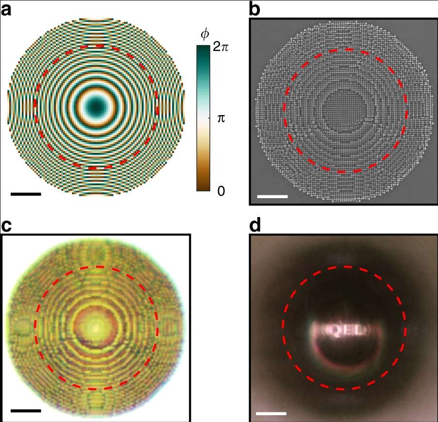
abstract = {Quantum emitters such as the diamond nitrogen-vacancy (NV) center are the basis for a wide range of quantum technologies. However, refraction and reflections at material interfaces impede photon collection, and the emitters’ atomic scale necessitates the use of free space optical measurement setups that prevent packaging of quantum devices. To overcome these limitations, we design and fabricate a metasurface composed of nanoscale diamond pillars that acts as an immersion lens to collect and collimate the emission of an individual NV center. The metalens exhibits a numerical aperture greater than 1.0, enabling efficient fiber-coupling of quantum emitters. This flexible design will lead to the miniaturization of quantum devices in a wide range of host materials and the development of metasurfaces that shape single-photon emission for coupling to optical cavities or route photons based on their quantum state.},

keywords = {},

pubstate = {published},

tppubtype = {article}

}
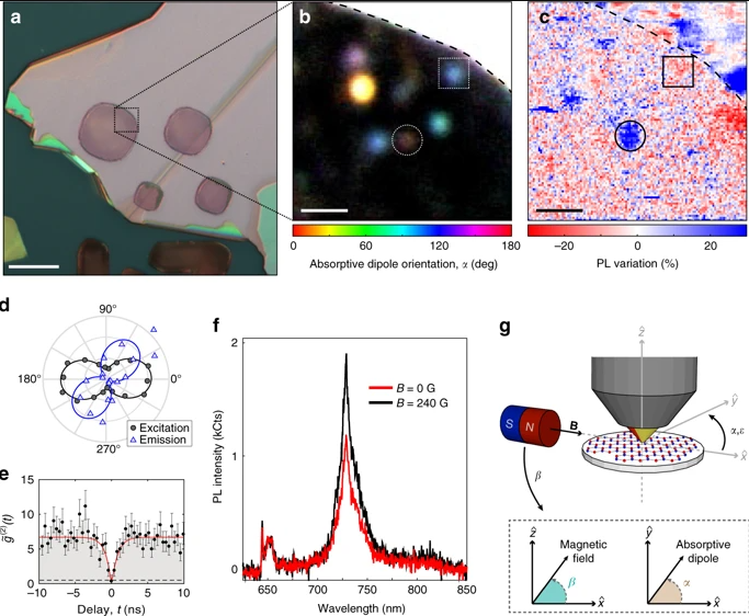
Exarhos, A L; Hopper, D A; Patel, R N; Doherty, M W; Bassett, L C
Magnetic-field-dependent quantum emission in hexagonal boron nitride at room temperature Journal Article
In: Nature Communications, vol. 10, no. 222, 2019.
@article{Exarhos2019,
title = {Magnetic-field-dependent quantum emission in hexagonal boron nitride at room temperature},
author = {A L Exarhos and D A Hopper and R N Patel and M W Doherty and L C Bassett},
url = {https://www.nature.com/articles/s41467-018-08185-8
https://www.nature.com/collections/rcdhyvxytb
https://spectrum.ieee.org/tech-talk/semiconductors/nanotechnology/qubits-and-nanosensors-in-a-2d-material
https://medium.com/penn-engineering/penn-engineers-develop-room-temperature-two-dimensional-platform-for-quantum-technology-cae3a5c0d8f9},
year = {2019},
date = {2019-01-15},
journal = {Nature Communications},
volume = {10},
number = {222},
abstract = {Selected as Editor's Highlight (linked)
Press coverage in IEEE Spectrum and Penn Medium (linked)
Optically addressable spins associated with defects in wide-bandgap semiconductors are versatile platforms for quantum information processing and nanoscale sensing, where spin-dependent inter-system crossing transitions facilitate optical spin initialization and readout. Recently, the van der Waals material hexagonal boron nitride (h-BN) has emerged as a robust host for quantum emitters, promising efficient photon extraction and atom-scale engineering, but observations of spin-related effects have remained thus far elusive. Here, we report room-temperature observations of strongly anisotropic photoluminescence patterns as a function of applied magnetic field for select quantum emitters in h-BN. Field-dependent variations in the steady-state photoluminescence and photon emission statistics are consistent with an electronic model featuring a spin-dependent inter-system crossing between triplet and singlet manifolds, indicating that optically-addressable spin defects are present in h-BN.},
keywords = {},
pubstate = {published},
tppubtype = {article}
}
Press coverage in IEEE Spectrum and Penn Medium (linked)
Optically addressable spins associated with defects in wide-bandgap semiconductors are versatile platforms for quantum information processing and nanoscale sensing, where spin-dependent inter-system crossing transitions facilitate optical spin initialization and readout. Recently, the van der Waals material hexagonal boron nitride (h-BN) has emerged as a robust host for quantum emitters, promising efficient photon extraction and atom-scale engineering, but observations of spin-related effects have remained thus far elusive. Here, we report room-temperature observations of strongly anisotropic photoluminescence patterns as a function of applied magnetic field for select quantum emitters in h-BN. Field-dependent variations in the steady-state photoluminescence and photon emission statistics are consistent with an electronic model featuring a spin-dependent inter-system crossing between triplet and singlet manifolds, indicating that optically-addressable spin defects are present in h-BN.
2018
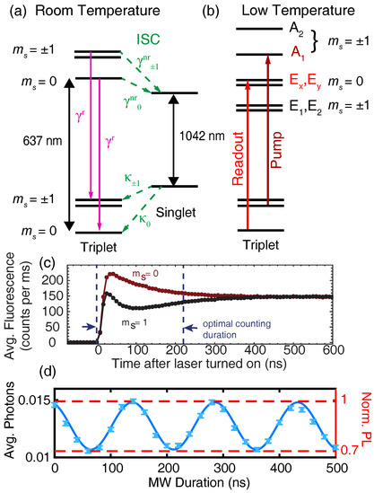
Hopper, D A; Shulevitz, H J; Bassett, L C
Spin readout techniques of the nitrogen-vacancy center in diamond Journal Article
In: Micromachines, vol. 9, pp. 437, 2018.
@article{Hopper2018,

title = {Spin readout techniques of the nitrogen-vacancy center in diamond},

author = {D A Hopper and H J Shulevitz and L C Bassett},

url = {https://www.mdpi.com/2072-666X/9/9/437},

year  = {2018},

date = {2018-08-30},

journal = {Micromachines},

volume = {9},

pages = {437},

abstract = {The diamond nitrogen-vacancy (NV) center is a leading platform for quantum information science due to its optical addressability and room-temperature spin coherence. However, measurements of the NV center’s spin state typically require averaging over many cycles to overcome noise. Here, we review several approaches to improve the readout performance and highlight future avenues of research that could enable single-shot electron-spin readout at room temperature.},

keywords = {},

pubstate = {published},

tppubtype = {article}

}
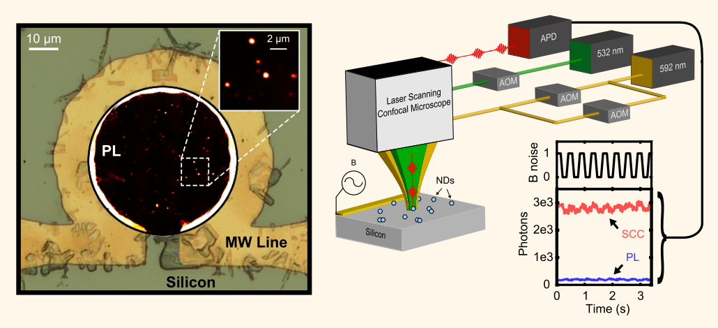
Hopper, D A; Grote, R R; Parks, S M; Bassett, L C
Amplified sensitivity of nitrogen-vacancy spins in nanodiamonds using all-optical charge readout Journal Article
In: ACS Nano, vol. 12, pp. 4678-4686, 2018.
@article{Hopper2018b,

title = {Amplified sensitivity of nitrogen-vacancy spins in nanodiamonds using all-optical charge readout},

author = {D A Hopper and R R Grote and S M Parks and L C Bassett},

url = {https://pubs.acs.org/doi/10.1021/acsnano.8b01265


https://arxiv.org/abs/1712.03882},

year  = {2018},

date = {2018-04-13},

journal = {ACS Nano},

volume = {12},

pages = {4678-4686},

abstract = {Nanodiamonds containing nitrogen-vacancy (NV) centers offer a versatile platform for sensing applications spanning from nanomagnetism to in vivo monitoring of cellular processes. In many cases, however, weak optical signals and poor contrast demand long acquisition times that prevent the measurement of environmental dynamics. Here, we demonstrate the ability to perform fast, high-contrast optical measurements of charge distributions in ensembles of NV centers in nanodiamonds and use the technique to improve the spin-readout signal-to-noise ratio through spin-to-charge conversion. A study of 38 nanodiamonds with sizes ranging between 20 and 70 nm, each hosting a small ensemble of NV centers, uncovers complex, multiple time scale dynamics due to radiative and nonradiative ionization and recombination processes. Nonetheless, the NV-containing nanodiamonds universally exhibit charge-dependent photoluminescence contrasts and the potential for enhanced spin readout using spin-to-charge conversion. We use the technique to speed up a T1 relaxometry measurement by a factor of 5.},

keywords = {},

pubstate = {published},

tppubtype = {article}

}
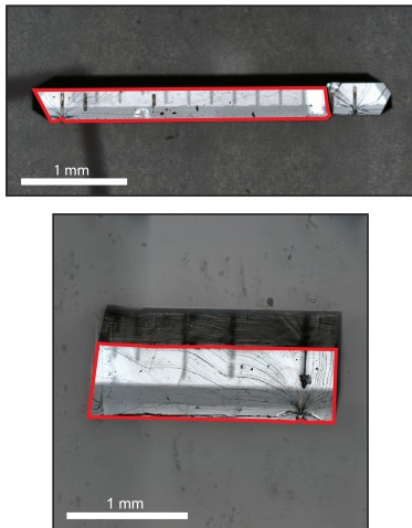
Parks, S M; Grote, R R; Hopper, D A; Bassett, L C
Fabrication of (111)-faced single-crystal diamond plates by laser nucleated cleaving Journal Article
In: Diamond and Related Materials, vol. 84, pp. 20-25, 2018.
@article{Parks2018,

title = {Fabrication of (111)-faced single-crystal diamond plates by laser nucleated cleaving},

author = {S M Parks and R R Grote and D A Hopper and L C Bassett},

url = {https://www.sciencedirect.com/science/article/pii/S0925963517307136?via%3Dihub


https://arxiv.org/abs/1712.03882},

year  = {2018},

date = {2018-02-28},

journal = {Diamond and Related Materials},

volume = {84},

pages = {20-25},

abstract = {Single-crystal diamond plates with surfaces oriented in a (111) crystal plane are required for high-performance solid-state device platforms ranging from power electronics to quantum information processing architectures. However, producing plates with this orientation has proven challenging. In this paper, we demonstrate a method for reliably and precisely fabricating (111)-faced plates from commercially available, chemical-vapor-deposition-grown, type-IIa single-crystal diamond substrates with (100) faces. Our method uses a nanosecond-pulsed visible laser to nucleate and propagate a mechanical cleave in a chosen (111) crystal plane, resulting in faces as large as 3.0mm × 0.3mm with atomically flat surfaces, negligible miscut angles, and near zero kerf loss. We discuss the underlying physical mechanisms of the process along with potential improvements that will enable the production of millimeter-scale (111)-faced single-crystal diamond plates for a variety of emerging devices and applications.},

keywords = {},

pubstate = {published},

tppubtype = {article}

}
2017
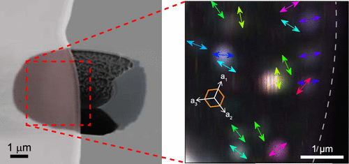
Exarhos, A L; Hopper, D A; Grote, R R; Alkauskas, A; Bassett, L C
Optical signatures of quantum emitters in suspended hexagonal boron nitride Journal Article
In: ACS Nano, vol. 11, pp. 3328-3336, 2017.
@article{Exarhos2017,

title = {Optical signatures of quantum emitters in suspended hexagonal boron nitride},

author = {A L Exarhos and D A Hopper and R R Grote and A Alkauskas and L C Bassett},

url = {https://pubs.acs.org/doi/abs/10.1021/acsnano.7b00665},

year  = {2017},

date = {2017-03-07},

journal = {ACS Nano},

volume = {11},

pages = {3328-3336},

abstract = {Hexagonal boron nitride (h-BN) is rapidly emerging as an attractive material for solid-state quantum engineering. Analogously to three-dimensional wide-band-gap semiconductors such as diamond, h-BN hosts isolated defects exhibiting visible fluorescence at room temperature, and the ability to position such quantum emitters within a two-dimensional material promises breakthrough advances in quantum sensing, photonics, and other quantum technologies. Critical to such applications is an understanding of the physics underlying h-BN’s quantum emission. We report the creation and characterization of visible single-photon sources in suspended, single-crystal, h-BN films. With substrate interactions eliminated, we study the spectral, temporal, and spatial characteristics of the defects’ optical emission. Theoretical analysis of the defects’ spectra reveals similarities in vibronic coupling to h-BN phonon modes despite widely varying fluorescence wavelengths, and a statistical analysis of the polarized emission from many emitters throughout the same single-crystal flake uncovers a weak correlation between the optical dipole orientations of some defects and h-BN’s primitive crystallographic axes, despite a clear misalignment for other dipoles. These measurements constrain possible defect models and, moreover, suggest that several classes of emitters can exist simultaneously throughout free-standing h-BN, whether they be different defects, different charge states of the same defect, or the result of strong local perturbations.},

keywords = {},

pubstate = {published},

tppubtype = {article}

}
2016
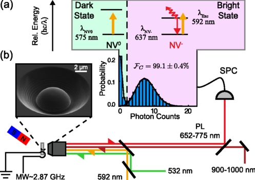
Hopper, D A; Grote, R R; Exarhos, A L; Bassett, L C
Near-infrared-assisted charge control and spin readout of the nitrogen-vacancy center in diamond Journal Article
In: Physical Review B, vol. 94, pp. 241201, 2016.
@article{Hopper2016,

title = {Near-infrared-assisted charge control and spin readout of the nitrogen-vacancy center in diamond},

author = {D A Hopper and R R Grote and A L Exarhos and L C Bassett},

url = {https://journals.aps.org/prb/abstract/10.1103/PhysRevB.94.241201},

year  = {2016},

date = {2016-12-09},

journal = {Physical Review B},

volume = {94},

pages = {241201},

abstract = {We utilize nonlinear absorption to design all-optical protocols that improve both charge-state initialization and spin readout for the nitrogen-vacancy (NV) center in diamond. Nonmonotonic variations in the equilibrium charge state as a function of visible and near-infrared optical power are attributed to competing multiphoton absorption processes. In certain regimes, multicolor illumination enhances the steady-state population of the NV's negative charge state above 90%. At higher NIR intensities, selective ionization of the singlet manifold facilitates a protocol for spin-to-charge conversion that dramatically enhances the spin readout fidelity. We demonstrate a sixfold increase in the signal-to-noise ratio for single-shot spin measurements and demonstrate a pathway towards single-shot electron spin readout at room temperature.},

keywords = {},

pubstate = {published},

tppubtype = {article}

}
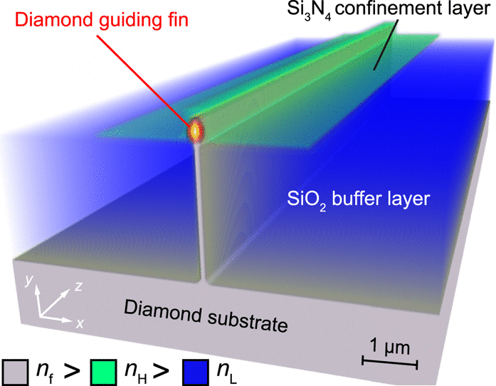
Grote, R R; Bassett, L C
Single-mode optical waveguides on native high-refractive-index substrates Journal Article
In: APL Photonics, vol. 1, pp. 071302, 2016.
@article{Grote2016,

title = {Single-mode optical waveguides on native high-refractive-index substrates},

author = {R R Grote and L C Bassett},

url = {https://aip.scitation.org/doi/10.1063/1.4955065},

year  = {2016},

date = {2016-08-01},

journal = {APL Photonics},

volume = {1},

pages = {071302},

abstract = {High-refractive-index semiconductor optical waveguides form the basis for modern photonic integrated circuits (PICs). However, conventional methods for achieving optical confinement require a thick lower-refractive-index support layer that impedes large-scale co-integration with electronics and limits the materials on which PICs can be fabricated. To address this challenge, we present a general architecture for single-mode waveguides that confine light in a high-refractive-index material on a native substrate. The waveguide consists of a high-aspect-ratio fin of the guiding material surrounded by lower-refractive-index dielectrics and is compatible with standard top-down fabrication techniques. This letter describes a physically intuitive, semi-analytical, effective index model for designing fin waveguides, which is confirmed with fully vectorial numerical simulations. Design examples are presented for diamond and silicon at visible and telecommunications wavelengths, respectively, along with calculations of propagation loss due to bending, scattering, and substrate leakage. Potential methods of fabrication are also discussed. The proposed waveguide geometry allows PICs to be fabricated alongside silicon CMOS electronics on the same wafer, removes the need for heteroepitaxy in III-V PICs, and will enable wafer-scale photonic integration on emerging material platforms such as diamond and SiC.},

keywords = {},

pubstate = {published},

tppubtype = {article}

}
2014
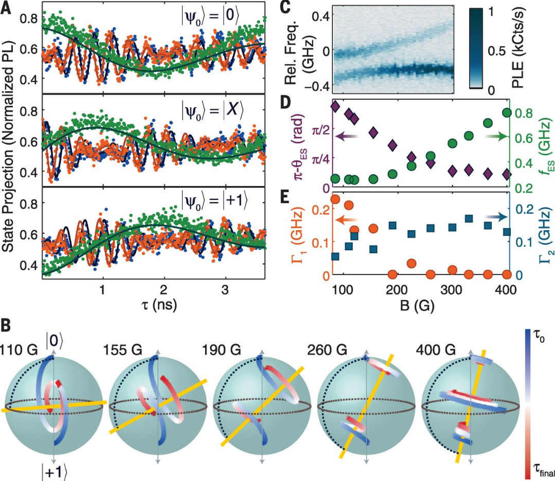
Bassett, L C; Heremans, F J; Christle, D J; Yale, C G; Burkard, G; Buckley, B B; Awschalom, D D
Ultrafast optical control of orbital and spin dynamics in a solid-state defect Journal Article
In: Science, vol. 345, pp. 1333-1337, 2014.
@article{Bassett2014,

title = {Ultrafast optical control of orbital and spin dynamics in a solid-state defect},

author = {L C Bassett and F J Heremans and D J Christle and C G Yale and G Burkard and B B Buckley and D D Awschalom},

url = {https://science.sciencemag.org/content/345/6202/1333},

year  = {2014},

date = {2014-09-12},

journal = {Science},

volume = {345},

pages = {1333-1337},

abstract = {Atom-scale defects in semiconductors are promising building blocks for quantum devices, but our understanding of their material-dependent electronic structure, optical interactions, and dissipation mechanisms is lacking. Using picosecond resonant pulses of light, we study the coherent orbital and spin dynamics of a single nitrogen-vacancy center in diamond over time scales spanning six orders of magnitude. We develop a time-domain quantum tomography technique to precisely map the defect’s excited-state Hamiltonian and exploit the excited-state dynamics to control its ground-state spin with optical pulses alone. These techniques generalize to other optically addressable nanoscale spin systems and serve as powerful tools to characterize and control spin qubits for future applications in quantum technology.},

keywords = {},

pubstate = {published},

tppubtype = {article}

}

Bassett, L C
Review: Quantum Mechanics with Applications to Nanotechnology and Information Science Miscellaneous
2014.
@misc{Bassett2014b,

title = {Review: Quantum Mechanics with Applications to Nanotechnology and Information Science},

author = {L C Bassett},

url = {https://physicstoday.scitation.org/doi/10.1063/PT.3.2451 http://www.amazon.com/gp/search?keywords=9780444537867&index=books&linkCode=qs&tag=physicstoday-20},

year  = {2014},

date = {2014-07-01},

abstract = {Quantum Mechanics with Applications to Nanotechnology and Information Science, Yehuda B. Band and Yshai Avishai, Academic Press, 2013. $126.00 (971 pp.). ISBN 978-0-444-53786-7


As we get better at controlling materials and fabricating devices on the atomic scale, we’ll need more “quantum engineers” to tackle the inherent challenges of technologies that exploit quantum effects. Although many modern devices rely on quantum mechanics in one way or another—for example, on population inversion in lasers or electron tunneling in transistors—most of those quantum effects can be described semiclassically and are accessible to engineers who have taken the standard courses on solid-state devices.},

keywords = {},

pubstate = {published},

tppubtype = {misc}

}
As we get better at controlling materials and fabricating devices on the atomic scale, we’ll need more “quantum engineers” to tackle the inherent challenges of technologies that exploit quantum effects. Although many modern devices rely on quantum mechanics in one way or another—for example, on population inversion in lasers or electron tunneling in transistors—most of those quantum effects can be described semiclassically and are accessible to engineers who have taken the standard courses on solid-state devices.
2007
test, (Ed.)
teset Journal Article
In: test, vol. 1, no. 1, pp. 1, 2007.
@article{,

title = {teset},

editor = {test},

year  = {2007},

date = {2007-05-08},

journal = {test},

volume = {1},

number = {1},

pages = {1},

abstract = {test},

keywords = {},

pubstate = {published},

tppubtype = {article}

}
Select publications before 2014
- “All-optical control of a solid-state spin using coherent dark states”, C. G. Yale, B. B. Buckley, D. J. Christle, G. Burkard, F. J. Heremans, L. C. Bassett, and D. D. Awschalom, Proc. Natl. Acad. Sci. USA 110, 7595 (2013).
- “Quantum spintronics: Engineering and manipulating atom-like spins in semiconductors”, D.D. Awschalom, L.C. Bassett, A.S. Dzurak, E.L. Hu and J.R. Petta, Science 339, 1174 (2013).
Related article: “The Future of Quantum Information Processing”, J. Stajic, Science 339, 1163 (2013).
- “Engineering and quantum control of single spins in semiconductors”, D.M. Toyli, L.C. Bassett, B.B. Buckley, G. Calusine and D.D. Awschalom, MRS Bulletin 38, 139 (2013).
- “Engineering shallow spins in diamond with nitrogen delta-doping”, K. Ohno, F. J. Heremans, L. C. Bassett, B. A. Myers, D. M. Toyli, A. C. Bleszynski-Jayich, C. J. Palmstrøm, and D. D. Awschalom, Appl. Phys. Lett. 101, 082413 (2012).
- “Electrical tuning of single nitrogen-vacancy center optical transitions enhanced by photoinduced fields”, L. C. Bassett, F. J. Heremans, C. G. Yale, B. B. Buckley, and D. D. Awschalom, Phys. Rev. Lett. 107, 266403 (2011).
- “Spin-light coherence for single-spin measurement and control in diamond”, B. B. Buckley, G. D. Fuchs, L. C. Bassett, and D. D. Awschalom, Science 330, 1212 (2010).
Related article: “Quantum measurement and control of single spins in diamond”, Science 330, 1188 (2010).
