Quantum Control
Atom-scale impurities in solids can trap individual electrons, forming analogs of molecules in free space. Particularly in wide-bandgap semiconductors like diamond, the quantum coherence of such trapped electron spins can be remarkably long lived, even at room temperature, and individual defect spins can be controlled using optics and electronics. A prime example is the nitrogen-vacancy (NV) center in diamond, which shows promise as an optically-addressable quantum bit in future technologies for quantum information processing and nanoscale sensing. Harnessing the versatility of semiconductor fabrication technology, we aim to realize practical implementations of quantum technologies based on such systems.
Huang, Tzu-Yung; Hopper, David A.; Omirzakhov, Kaisarbek; Idjadi, Mohamad Hossein; Breitweiser, S. Alexander; Aflatouni, Firooz; Bassett, Lee C.
Electronic Noise Considerations for Designing Integrated Solid-State Quantum Memories Journal Article
In: Advanced Quantum Technologies, pp. 2400472, 2025.
@article{Huang2025,

title = {Electronic Noise Considerations for Designing Integrated Solid-State Quantum Memories},

author = {Tzu-Yung Huang and David A. Hopper and Kaisarbek Omirzakhov and Mohamad Hossein Idjadi and S. Alexander Breitweiser and Firooz Aflatouni and Lee C. Bassett},

url = {https://onlinelibrary.wiley.com/doi/10.1002/qute.202400472#

https://arxiv.org/abs/2501.00683},

year  = {2025},

date = {2025-02-06},

urldate = {2025-02-06},

journal = {Advanced Quantum Technologies},

pages = {2400472},

abstract = {As quantum networks expand and are deployed outside research laboratories, a need arises to design and integrate compact control electronics for each memory node. It is essential to understand the performance requirements for such systems, especially concerning tolerable levels of noise, since these specifications dramatically affect a system's design complexity and cost. Here, using an approach that can be easily generalized across quantum-hardware platforms, a case study based on nitrogen-vacancy (NV) centers in diamond is presented. The effects of phase noise and timing jitter in the control system in conjunction are modeled and experimentally verified with the spin qubit's environmental noise. The impact of different phase noise characteristics on the fidelity of dynamical decoupling sequences is also considered. The results demonstrate a procedure to specify design requirements for integrated quantum control signal generators for solid-state spin qubits, depending on their coherence time, intrinsic noise spectrum, and required fidelity.},

keywords = {},

pubstate = {published},

tppubtype = {article}

}
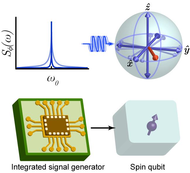
As quantum networks expand and are deployed outside research laboratories, a need arises to design and integrate compact control electronics for each memory node. It is essential to understand the performance requirements for such systems, especially concerning tolerable levels of noise, since these specifications dramatically affect a system's design complexity and cost. Here, using an approach that can be easily generalized across quantum-hardware platforms, a case study based on nitrogen-vacancy (NV) centers in diamond is presented. The effects of phase noise and timing jitter in the control system in conjunction are modeled and experimentally verified with the spin qubit's environmental noise. The impact of different phase noise characteristics on the fidelity of dynamical decoupling sequences is also considered. The results demonstrate a procedure to specify design requirements for integrated quantum control signal generators for solid-state spin qubits, depending on their coherence time, intrinsic noise spectrum, and required fidelity.
Patel, Raj N.; Fishman, Rebecca E. K.; Huang, Tzu-Yung; Gusdorff, Jordan A.; Fehr, David A.; Hopper, David A.; Breitweiser, S. Alex; Porat, Benjamin; Flatté, Michael E.; Bassett, Lee C.
Room Temperature Dynamics of an Optically Addressable Single Spin in Hexagonal Boron Nitride Journal Article
In: Nano Letters, vol. 24, iss. 25, pp. 7623-7628, 2024.
@article{Patel2024,

title = {Room Temperature Dynamics of an Optically Addressable Single Spin in Hexagonal Boron Nitride},

author = {Raj N. Patel and Rebecca E. K. Fishman and Tzu-Yung Huang and Jordan A. Gusdorff and David A. Fehr and David A. Hopper and S. Alex Breitweiser and Benjamin Porat and Michael E. Flatté and Lee C. Bassett},

url = {https://pubs.acs.org/doi/abs/10.1021/acs.nanolett.4c01333

https://arxiv.org/abs/2309.05604},

doi = {10.1021/acs.nanolett.4c01333},

year  = {2024},

date = {2024-06-11},

urldate = {2024-06-11},

journal = {Nano Letters},

volume = {24},

issue = {25},

pages = {7623-7628},

abstract = {Hexagonal boron nitride (h-BN) hosts pure single-photon emitters that have shown evidence of optically detected electronic spin dynamics. However, the electrical and chemical structures of these optically addressable spins are unknown, and the nature of their spin-optical interactions remains mysterious. Here, we use time-domain optical and microwave experiments to characterize a single emitter in h-BN exhibiting room temperature optically detected magnetic resonance. Using dynamical simulations, we constrain and quantify transition rates in the model, and we design optical control protocols that optimize the signal-to-noise ratio for spin readout. This constitutes a necessary step toward quantum control of spin states in h-BN.},

keywords = {},

pubstate = {published},

tppubtype = {article}

}
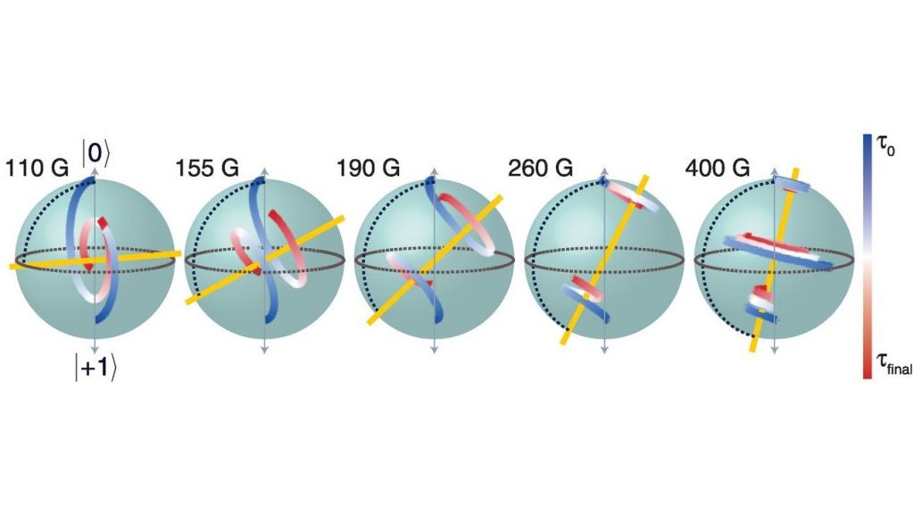
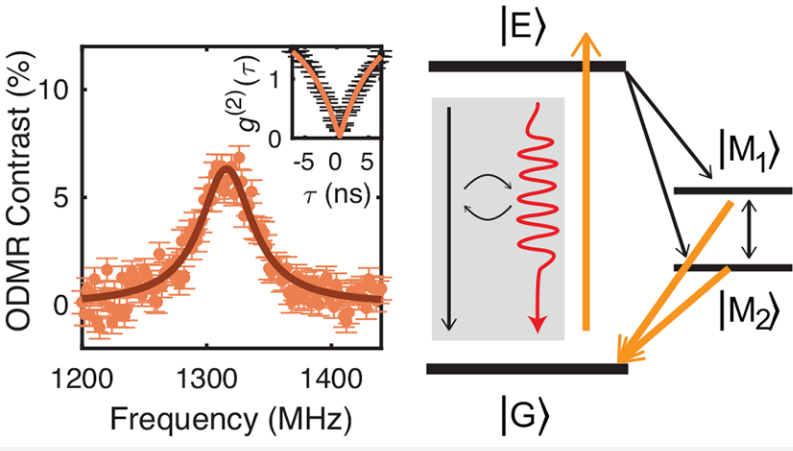
Hexagonal boron nitride (h-BN) hosts pure single-photon emitters that have shown evidence of optically detected electronic spin dynamics. However, the electrical and chemical structures of these optically addressable spins are unknown, and the nature of their spin-optical interactions remains mysterious. Here, we use time-domain optical and microwave experiments to characterize a single emitter in h-BN exhibiting room temperature optically detected magnetic resonance. Using dynamical simulations, we constrain and quantify transition rates in the model, and we design optical control protocols that optimize the signal-to-noise ratio for spin readout. This constitutes a necessary step toward quantum control of spin states in h-BN.
Sensing and Imaging
Highly localized, optically controllable spins can serve as remote sensors of their nanoscale environment, providing detailed information about their local conditions such as magnetic and electric fields, crystal strain, and temperature. This capability suggests many exciting applications, particularly in materials science, chemistry, and biology, where the ability to monitor fields and their dynamics on nanometer length scales could lead to breakthroughs in understanding protein dynamics, cellular communication, and complex quantum materials. We are developing quantum sensing applications and integrated quantum sensing platforms based on spins in solids.
Breitweiser, S. Alex; Ouellet, Mathieu; Huang, Tzu-Yung; Taminiau, Tim H.; Bassett, Lee C.
Quadrupolar resonance spectroscopy of individual nuclei using a room-temperature quantum sensor Journal Article
In: Nano Letters, vol. 24, iss. 51, pp. 16253-16260, 2024.
@article{Breitweiser2024,

title = {Quadrupolar resonance spectroscopy of individual nuclei using a room-temperature quantum sensor},

author = {S. Alex Breitweiser and Mathieu Ouellet and Tzu-Yung Huang and Tim H. Taminiau and Lee C. Bassett},

url = {https://pubs.acs.org/doi/abs/10.1021/acs.nanolett.4c04112

https://arxiv.org/abs/2405.14859},

year  = {2024},

date = {2024-12-12},

urldate = {2024-12-12},

journal = {Nano Letters},

volume = {24},

issue = {51},

pages = {16253-16260},

abstract = {Nuclear quadrupolar resonance (NQR) spectroscopy reveals chemical bonding patterns in materials and molecules through the unique coupling between nuclear spins and local fields. However, traditional NQR techniques require macroscopic ensembles of nuclei to yield a detectable signal, which obscures molecule-to-molecule variations. Solid-state spin qubits, such as the nitrogen-vacancy (NV) center in diamond, facilitate the detection and control of individual nuclei through their local magnetic couplings. Here, we use NV centers to perform NQR spectroscopy on their associated nitrogen-14 (14N) nuclei at room temperature. In mapping the nuclear quadrupolar Hamiltonian, we resolve minute variations between individual nuclei. The measurements reveal correlations between the Hamiltonian parameters associated with the NV center’s electronic and nuclear spin states, as well as a previously unreported symmetry-breaking quadrupolar term. We further design pulse sequences to initialize, read out, and control the quantum evolution of the 14N nuclear state using the nuclear quadrupolar Hamiltonian.},

keywords = {},

pubstate = {published},

tppubtype = {article}

}
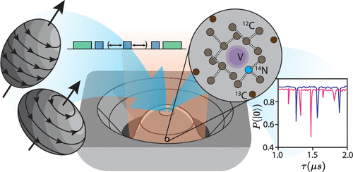
Nuclear quadrupolar resonance (NQR) spectroscopy reveals chemical bonding patterns in materials and molecules through the unique coupling between nuclear spins and local fields. However, traditional NQR techniques require macroscopic ensembles of nuclei to yield a detectable signal, which obscures molecule-to-molecule variations. Solid-state spin qubits, such as the nitrogen-vacancy (NV) center in diamond, facilitate the detection and control of individual nuclei through their local magnetic couplings. Here, we use NV centers to perform NQR spectroscopy on their associated nitrogen-14 (14N) nuclei at room temperature. In mapping the nuclear quadrupolar Hamiltonian, we resolve minute variations between individual nuclei. The measurements reveal correlations between the Hamiltonian parameters associated with the NV center’s electronic and nuclear spin states, as well as a previously unreported symmetry-breaking quadrupolar term. We further design pulse sequences to initialize, read out, and control the quantum evolution of the 14N nuclear state using the nuclear quadrupolar Hamiltonian.
Shulevitz, Henry J.; Amirshaghaghi, Ahmad; Ouellet, Mathieu; Brustoloni, Caroline; Yang, Shengsong; Ng, Jonah J.; Huang, Tzu-Yung; Jishkariani, Davit; Murray, Christopher B.; Tsourkas, Andrew; Kagan, Cherie R.; Bassett, Lee C.
Nanodiamond emulsions for enhanced quantum sensing and click-chemistry conjugation Journal Article
In: ACS Applied Nano Materials, vol. 7, iss. 13, pp. 15334-15343, 2024.
@article{Shulevitz2024,

title = {Nanodiamond emulsions for enhanced quantum sensing and click-chemistry conjugation},

author = {Henry J. Shulevitz and Ahmad Amirshaghaghi and Mathieu Ouellet and Caroline Brustoloni and Shengsong Yang and Jonah J. Ng and Tzu-Yung Huang and Davit Jishkariani and Christopher B. Murray and Andrew Tsourkas and Cherie R. Kagan and Lee C. Bassett},

url = {https://pubs.acs.org/doi/abs/10.1021/acsanm.4c01699

https://arxiv.org/abs/2311.16530},

doi = {10.1021/acsanm.4c01699},

year  = {2024},

date = {2024-06-29},

urldate = {2024-06-29},

journal = {ACS Applied Nano Materials},

volume = {7},

issue = {13},

pages = {15334-15343},

abstract = {Nanodiamonds containing nitrogen-vacancy (NV) centers can serve as colloidal quantum sensors of local fields in biological and chemical environments. However, nanodiamond surfaces are challenging to modify without degrading their colloidal stability or the NV center’s optical and spin properties. We present a simple and general method to coat nanodiamonds with a thin emulsion layer that preserves their quantum features, maintains their colloidal stability, and provides functional groups for subsequent cross-linking and click-chemistry conjugation reactions. To demonstrate this technique, we decorated nanodiamonds with combinations of carboxyl- and azide-terminated amphiphiles that enable conjugation using two different strategies. A theoretical model is developed to understand the effect of the emulsion layer on the NV center’s spin lifetime, and T1 relaxometry is employed to quantify the nanodiamonds’ chemical sensitivity to paramagnetic ions. This general approach to nanodiamond surface functionalization will enable advances in quantum nanomedicine and biological sensing.},

keywords = {},

pubstate = {published},

tppubtype = {article}

}
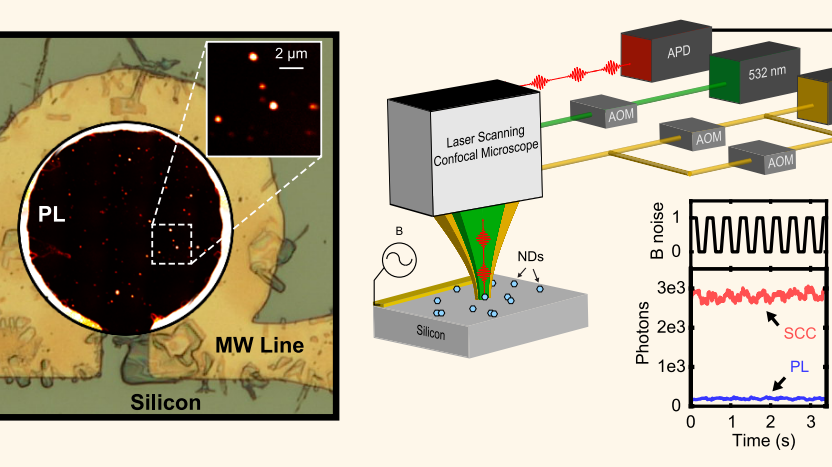
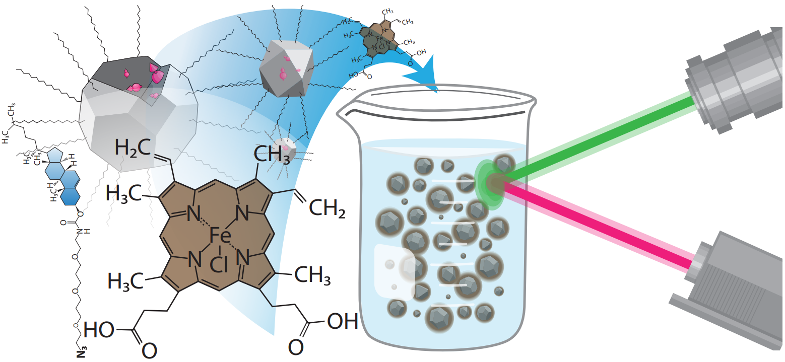
Nanodiamonds containing nitrogen-vacancy (NV) centers can serve as colloidal quantum sensors of local fields in biological and chemical environments. However, nanodiamond surfaces are challenging to modify without degrading their colloidal stability or the NV center’s optical and spin properties. We present a simple and general method to coat nanodiamonds with a thin emulsion layer that preserves their quantum features, maintains their colloidal stability, and provides functional groups for subsequent cross-linking and click-chemistry conjugation reactions. To demonstrate this technique, we decorated nanodiamonds with combinations of carboxyl- and azide-terminated amphiphiles that enable conjugation using two different strategies. A theoretical model is developed to understand the effect of the emulsion layer on the NV center’s spin lifetime, and T1 relaxometry is employed to quantify the nanodiamonds’ chemical sensitivity to paramagnetic ions. This general approach to nanodiamond surface functionalization will enable advances in quantum nanomedicine and biological sensing.
New Materials
Point defects in wide bandgap semiconductors, like the NV center in diamond, have emerged as leading platforms for quantum technologies, providing optically and electronically addressable spin states that are robust to environmental noise. However, identification of new defect systems in new host materials is generally a slow, ad hoc process. Because the desired operating parameters for these defect systems are application-specific and depend heavily on the materials involved, we are focused on combining new computational and experimental techniques to accelerate the discovery of defect-host systems that are optimized for spin-light quantum interfaces.
Quantum-mechanical effects become progressively more important in materials with reduced dimensions, offering both a challenge for the continued miniaturization of traditional electronics and an opportunity for developing new quantum technologies. Our group combines optical and electrical techniques to study new materials systems in both bulk and low-dimensional (0D, 1D, 2D) samples, particularly in semiconducting “beyond-carbon” materials such as boron nitride. These emerging materials offer many of the appealing features of their carbon counterparts but with additional advantages, particularly for optical measurements. We are interested in both the fundamental physics of these materials and their potential as electrical & optical components, sensors, and in quantum information technology.
Gusdorff, Jordan A.; Bhatia, Pia; Shin, Trey T.; Uy-Tioco, Alexandra Sofia; Sailors, Benjamin N.; Keneipp, Rachael N.; Drndić, Marija; Bassett, Lee C.
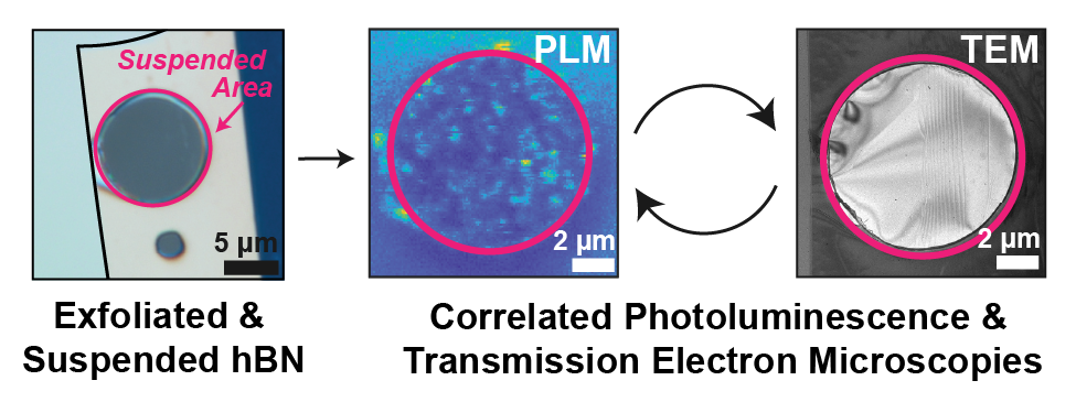
Correlated Structural and Optical Characterization of Hexagonal Boron Nitride Journal Article
In: ACS Nano, vol. 9, iss. 11, pp. 11100-11110, 2025.
@article{Gusdorff2025,

title = {Correlated Structural and Optical Characterization of Hexagonal Boron Nitride},

author = {Jordan A. Gusdorff and Pia Bhatia and Trey T. Shin and Alexandra Sofia Uy-Tioco and Benjamin N. Sailors and Rachael N. Keneipp and Marija Drndić and Lee C. Bassett},

url = {https://pubs.acs.org/doi/10.1021/acsnano.4c17676

https://arxiv.org/abs/2411.14408},

doi = {10.1021/acsnano.4c17676},

year  = {2025},

date = {2025-02-21},

urldate = {2025-02-21},

journal = {ACS Nano},

volume = {9},

issue = {11},

pages = {11100-11110},

abstract = {Hexagonal boron nitride (hBN) hosts quantum emitters that exhibit single-photon emission and spin-dependent fluorescence at room temperature. These features make hBN a promising platform for quantum sensing and photonics. Despite many investigations of their optical properties, the emitters' chemical structure remains unclear, as does the role of contamination at surfaces and interfaces in forming the emitters or modifying their properties. We prepare hBN samples that are compatible with both confocal photoluminescence microscopy (PL) and transmission electron microscopy (TEM), and we use those techniques to investigate correlations between fluorescent emission, flake morphology, and surface residue. We find that the microscopy techniques themselves induce changes in hBN's optical activity and residue morphology: PL measurements induce photobleaching, whereas TEM measurements alter surface residue and emission characteristics. We also study the effects of common treatments — annealing and oxygen plasma cleaning — on the structure and optical activity of hBN. The results illustrate the power and importance of correlative studies to elucidate aspects of microscopic mechanisms that influence hBN's functionality as a host for quantum emitters and spin defects.},

keywords = {},

pubstate = {published},

tppubtype = {article}

}
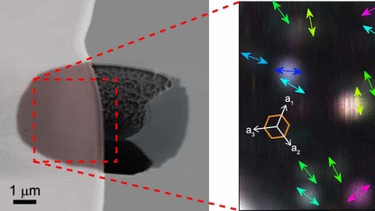
Hexagonal boron nitride (hBN) hosts quantum emitters that exhibit single-photon emission and spin-dependent fluorescence at room temperature. These features make hBN a promising platform for quantum sensing and photonics. Despite many investigations of their optical properties, the emitters' chemical structure remains unclear, as does the role of contamination at surfaces and interfaces in forming the emitters or modifying their properties. We prepare hBN samples that are compatible with both confocal photoluminescence microscopy (PL) and transmission electron microscopy (TEM), and we use those techniques to investigate correlations between fluorescent emission, flake morphology, and surface residue. We find that the microscopy techniques themselves induce changes in hBN's optical activity and residue morphology: PL measurements induce photobleaching, whereas TEM measurements alter surface residue and emission characteristics. We also study the effects of common treatments — annealing and oxygen plasma cleaning — on the structure and optical activity of hBN. The results illustrate the power and importance of correlative studies to elucidate aspects of microscopic mechanisms that influence hBN's functionality as a host for quantum emitters and spin defects.
Thompson, Sarah M.; Şahin, Cüneyt; Yang, Shengsong; Flatté, Michael E.; Murray, Christopher B.; Bassett, Lee C.; Kagan, Cherie R.
Red Emission from Copper-Vacancy Color Centers in Zinc Sulfide Colloidal Nanocrystals Journal Article
In: ACS Nano, 2023.
@article{Thompson2023,
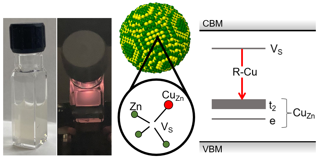
title = {Red Emission from Copper-Vacancy Color Centers in Zinc Sulfide Colloidal Nanocrystals},
author = {Sarah M. Thompson and Cüneyt Şahin and Shengsong Yang and Michael E. Flatté and Christopher B. Murray and Lee C. Bassett and Cherie R. Kagan},
url = {https://pubs.acs.org/doi/full/10.1021/acsnano.3c00191
https://arxiv.org/abs/2301.04223},
doi = {10.1021/acsnano.3c00191},
year = {2023},
date = {2023-03-09},
journal = {ACS Nano},
abstract = {Copper-doped zinc sulfide (ZnS:Cu) exhibits down-conversion luminescence in the UV, visible, and IR regions of the electromagnetic spectrum; the visible red, green, and blue emission is referred to as R-Cu, G-Cu, and B-Cu, respectively. The sub-bandgap emission arises from optical transitions between localized electronic states created by point defects, making ZnS:Cu a prolific phosphor material and an intriguing candidate material for quantum information science, where point defects excel as single-photon sources and spin qubits. Colloidal nanocrystals (NCs) of ZnS:Cu are particularly interesting as hosts for the creation, isolation, and measurement of quantum defects, since their size, composition, and surface chemistry can be precisely tailored for bio-sensing and opto-electronic applications. Here, we present a method for synthesizing colloidal ZnS:Cu NCs that emit primarily R-Cu, which has been proposed to arise from the CuZn-VS complex, an impurity-vacancy point defect structure analogous to well-known quantum defects in other materials that produce favorable optical and spin dynamics. First principles calculations confirm the thermodynamic stability and electronic structure of CuZn-VS. Temperature- and time-dependent optical properties of ZnS:Cu NCs show blueshifting luminescence and an anomalous plateau in the intensity dependence as temperature is increased from 19 K to 290 K, for which we propose an empirical dynamical model based on thermally-activated coupling between two manifolds of states inside the ZnS bandgap. Understanding of R-Cu emission dynamics, combined with a controlled synthesis method for obtaining R-Cu centers in colloidal NC hosts, will greatly facilitate the development of CuZn-VS and related complexes as quantum point defects in ZnS.},
keywords = {},
pubstate = {published},
tppubtype = {article}
}
Copper-doped zinc sulfide (ZnS:Cu) exhibits down-conversion luminescence in the UV, visible, and IR regions of the electromagnetic spectrum; the visible red, green, and blue emission is referred to as R-Cu, G-Cu, and B-Cu, respectively. The sub-bandgap emission arises from optical transitions between localized electronic states created by point defects, making ZnS:Cu a prolific phosphor material and an intriguing candidate material for quantum information science, where point defects excel as single-photon sources and spin qubits. Colloidal nanocrystals (NCs) of ZnS:Cu are particularly interesting as hosts for the creation, isolation, and measurement of quantum defects, since their size, composition, and surface chemistry can be precisely tailored for bio-sensing and opto-electronic applications. Here, we present a method for synthesizing colloidal ZnS:Cu NCs that emit primarily R-Cu, which has been proposed to arise from the CuZn-VS complex, an impurity-vacancy point defect structure analogous to well-known quantum defects in other materials that produce favorable optical and spin dynamics. First principles calculations confirm the thermodynamic stability and electronic structure of CuZn-VS. Temperature- and time-dependent optical properties of ZnS:Cu NCs show blueshifting luminescence and an anomalous plateau in the intensity dependence as temperature is increased from 19 K to 290 K, for which we propose an empirical dynamical model based on thermally-activated coupling between two manifolds of states inside the ZnS bandgap. Understanding of R-Cu emission dynamics, combined with a controlled synthesis method for obtaining R-Cu centers in colloidal NC hosts, will greatly facilitate the development of CuZn-VS and related complexes as quantum point defects in ZnS.
Quantum Photonics
The atomic scales and high refractive index environments of solid state quantum emitters prevent their detection without bulky free-space optical setups. Condensed optical tools will be required to replace these traditional setups in integrated devices that rely on solid state quantum emitters. An example of such a tool is the immersion metalens that our lab has fabricated and is now improving through fabrication-constrained inverse design techniques.

Klein, Amelia R.; Engheta, Nader; Bassett, Lee C.
Designing metasurface optical interfaces for solid-state qubits using many-body adjoint shape optimization Journal Article
In: Optics Express, vol. 32, iss. 22, pp. 38504-38515, 2024.
@article{Klein2024,

title = {Designing metasurface optical interfaces for solid-state qubits using many-body adjoint shape optimization},

author = {Amelia R. Klein and Nader Engheta and Lee C. Bassett},

url = {https://opg.optica.org/oe/fulltext.cfm?uri=oe-32-22-38504&id=561330

https://arxiv.org/abs/2406.08212},

doi = {10.1364/OE.522501},

year  = {2024},

date = {2024-10-09},

urldate = {2024-10-09},

journal = {Optics Express},

volume = {32},

issue = {22},

pages = {38504-38515},

abstract = {We present a general strategy for the inverse design of metasurfaces composed of elementary shapes. We use it to design a structure that collects and collimates light from nitrogen-vacancy centers in diamond. Such metasurfaces constitute scalable optical interfaces for solid-state qubits, enabling efficient photon coupling into optical fibers and eliminating free-space collection optics. The many-body shape optimization strategy is a practical alternative to topology optimization that explicitly enforces material and fabrication constraints throughout the optimization, while still achieving high performance. The metasurface is easily adaptable to other solid-state qubits, and the optimization method is broadly applicable to fabrication-constrained photonic design problems.},

keywords = {},

pubstate = {published},

tppubtype = {article}

}
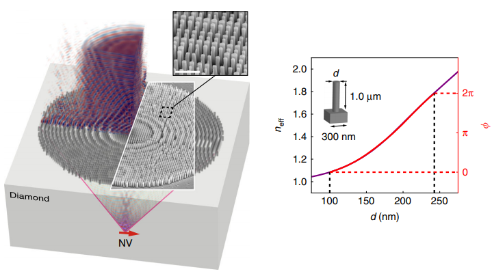
We present a general strategy for the inverse design of metasurfaces composed of elementary shapes. We use it to design a structure that collects and collimates light from nitrogen-vacancy centers in diamond. Such metasurfaces constitute scalable optical interfaces for solid-state qubits, enabling efficient photon coupling into optical fibers and eliminating free-space collection optics. The many-body shape optimization strategy is a practical alternative to topology optimization that explicitly enforces material and fabrication constraints throughout the optimization, while still achieving high performance. The metasurface is easily adaptable to other solid-state qubits, and the optimization method is broadly applicable to fabrication-constrained photonic design problems.