Quantum Engineering Laboratory
Our group studies quantum dynamics in nanoscale materials and devices using optics and electronics. We seek to better understand complex quantum-mechanical systems, with a goal of developing new technologies for communication, computation, and sensing based on quantum physics.


News
- Newton: Mimicking prions for self-replicating machines
Our paper on mechanically modeling prions is featured on Newton.
- EurekAlert!: New quantum sensing technology reveals sub-atomic signals
Our paper on nuclear quadrupolar resonance spectroscopy is featured on EurekAlert!
- Congratulations, Mathieu!
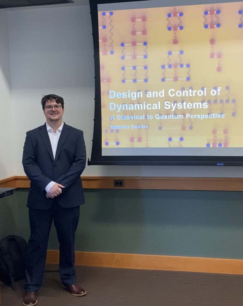
Congratulations to Mathieu on defending his PhD thesis!
Recent Publications
Minnella, Joseph D.; Ouellet, Mathieu; Klein, Amelia R.; Bassett, Lee C.
Single-gate, multipartite entanglement on a room-temperature quantum register Journal Article Forthcoming
In: arXiv, Forthcoming.
@article{Minnella2025,

title = {Single-gate, multipartite entanglement on a room-temperature quantum register},

author = {Joseph D. Minnella and Mathieu Ouellet and Amelia R. Klein and Lee C. Bassett},

url = {https://arxiv.org/abs/2508.08465},

year  = {2025},

date = {2025-08-11},

urldate = {2025-08-11},

journal = {arXiv},

abstract = {Multipartite entanglement is an essential aspect of quantum systems, needed to execute quantum algorithms, implement error correction, and achieve quantum-enhanced sensing. In solid-state quantum registers such nitrogen-vacancy (NV) centers in diamond, entangled states are typically created using sequential, pairwise gates between the central electron and individual nuclear qubits. This sequential approach is slow and suffers from crosstalk errors. Here, we demonstrate a parallelized multi-qubit entangling gate to generate a four-qubit GHZ state using a room-temperature NV center in only 14.8  s   10 times faster than using sequences of two-qubit gates. The entangled states are verified by measuring multiple quantum coherences. Two-qubit entangling gates have an average fidelity of 0.96(1), and the four-qubit parallel gate has a fidelity of 0.92(4), whereas the sequential four-qubit gate fidelity is only 0.69(3). The approach is generalizable to other solid-state platforms, and it lays the foundation for scalable generation and control of entanglement in practical devices. },

keywords = {},

pubstate = {forthcoming},

tppubtype = {article}

}
Ouellet, Mathieu; Bassett, Dani S.; Bassett, Lee C.; Murphy, Kieran A.; Patankar, Shubhankar P.
Mechanical prions as self-assembling microstructures Journal Article
In: Newton, vol. 1, iss. 5, pp. 100098, 2025.
@article{Ouellet2025,

title = {Mechanical prions as self-assembling microstructures},

author = {Mathieu Ouellet and Dani S. Bassett and Lee C. Bassett and Kieran A. Murphy and Shubhankar P. Patankar},

url = {https://www.cell.com/newton/fulltext/S2950-6360(25)00090-8

https://arxiv.org/abs/2402.10939},

year  = {2025},

date = {2025-07-07},

urldate = {2025-05-08},

journal = {Newton},

volume = {1},

issue = {5},

pages = {100098},

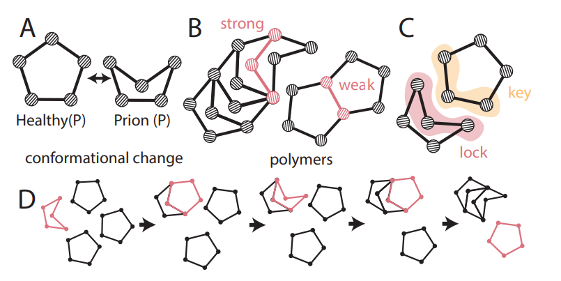
abstract = {Prions are misfolded proteins that transmit their structural arrangement to neighboring proteins. In biological systems, prion dynamics can produce a variety of complex functional outcomes. Yet, an understanding of prionic causes has been hampered by the fact that few computational models exist that allow for experimental design, hypothesis testing, and control. Here, we identify essential prionic properties and present a biologically inspired model of prions using simple mechanical structures capable of undergoing complex conformational change. We demonstrate the utility of our approach by designing a prototypical mechanical prion and validating its properties experimentally. Our work provides a design framework for harnessing and manipulating prionic properties in natural and artificial systems.},

keywords = {},

pubstate = {published},

tppubtype = {article}

}
Panfil, Yossef E.; Thompson, Sarah M.; Chen, Gary; Ng, Jonah; Kagan, Cherie R.; Bassett, Lee C.
Room-temperature quantum emission from CuZn-VS defects in ZnS:Cu colloidal nanocrystals Journal Article
In: ACS Nano, vol. 19, iss. 23, pp. 21400-21410, 2025.
@article{Panfil2025,

title = {Room-temperature quantum emission from CuZn-VS defects in ZnS:Cu colloidal nanocrystals},

author = {Yossef E. Panfil and Sarah M. Thompson and Gary Chen and Jonah Ng and Cherie R. Kagan and Lee C. Bassett},

url = {https://pubs.acs.org/doi/abs/10.1021/acsnano.5c01265

https://arxiv.org/abs/2501.11812},

year  = {2025},

date = {2025-06-05},

urldate = {2025-06-05},

journal = {ACS Nano},

volume = {19},

issue = {23},

pages = { 21400-21410},

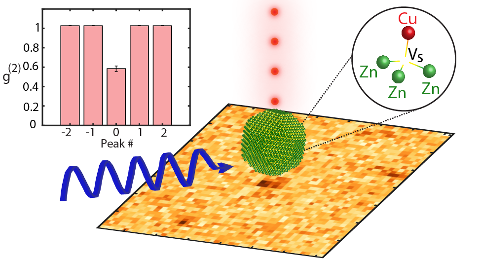
abstract = {We report room-temperature observations of CuZn-VS quantum emitters in individual ZnS:Cu nanocrystals (NCs). Using time-gated imaging, we isolate the distinct, ∼3-μs-long, red photoluminescence (PL) emission of CuZn-VS defects, enabling their precise identification and statistical characterization. The emitters exhibit distinct blinking and photon antibunching, consistent with individual NCs containing two to four CuZn-VS defects. The quantum emitters' PL spectra show a pronounced blue shift compared to NC dispersions, likely due to photochemical and charging effects. Emission polarization measurements of quantum emitters are consistent with a σ-character optical dipole transition and the symmetry of the CuZn-VS defect. These observations motivate further investigation of CuZn-VS defects in ZnS NCs for use in quantum technologies.},

keywords = {},

pubstate = {published},

tppubtype = {article}

}
Gusdorff, Jordan A.; Bhatia, Pia; Shin, Trey T.; Uy-Tioco, Alexandra Sofia; Sailors, Benjamin N.; Keneipp, Rachael N.; Drndić, Marija; Bassett, Lee C.
Correlated Structural and Optical Characterization of Hexagonal Boron Nitride Journal Article
In: ACS Nano, vol. 9, iss. 11, pp. 11100-11110, 2025.
@article{Gusdorff2025,

title = {Correlated Structural and Optical Characterization of Hexagonal Boron Nitride},

author = {Jordan A. Gusdorff and Pia Bhatia and Trey T. Shin and Alexandra Sofia Uy-Tioco and Benjamin N. Sailors and Rachael N. Keneipp and Marija Drndić and Lee C. Bassett},

url = {https://pubs.acs.org/doi/10.1021/acsnano.4c17676

https://arxiv.org/abs/2411.14408},

doi = {10.1021/acsnano.4c17676},

year  = {2025},

date = {2025-02-21},

urldate = {2025-02-21},

journal = {ACS Nano},

volume = {9},

issue = {11},

pages = {11100-11110},

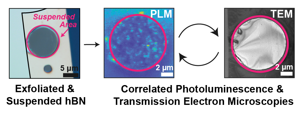
abstract = {Hexagonal boron nitride (hBN) hosts quantum emitters that exhibit single-photon emission and spin-dependent fluorescence at room temperature. These features make hBN a promising platform for quantum sensing and photonics. Despite many investigations of their optical properties, the emitters' chemical structure remains unclear, as does the role of contamination at surfaces and interfaces in forming the emitters or modifying their properties. We prepare hBN samples that are compatible with both confocal photoluminescence microscopy (PL) and transmission electron microscopy (TEM), and we use those techniques to investigate correlations between fluorescent emission, flake morphology, and surface residue. We find that the microscopy techniques themselves induce changes in hBN's optical activity and residue morphology: PL measurements induce photobleaching, whereas TEM measurements alter surface residue and emission characteristics. We also study the effects of common treatments — annealing and oxygen plasma cleaning — on the structure and optical activity of hBN. The results illustrate the power and importance of correlative studies to elucidate aspects of microscopic mechanisms that influence hBN's functionality as a host for quantum emitters and spin defects.},

keywords = {},

pubstate = {published},

tppubtype = {article}

}
Huang, Tzu-Yung; Hopper, David A.; Omirzakhov, Kaisarbek; Idjadi, Mohamad Hossein; Breitweiser, S. Alexander; Aflatouni, Firooz; Bassett, Lee C.
Electronic Noise Considerations for Designing Integrated Solid-State Quantum Memories Journal Article
In: Advanced Quantum Technologies, pp. 2400472, 2025.
@article{Huang2025,

title = {Electronic Noise Considerations for Designing Integrated Solid-State Quantum Memories},

author = {Tzu-Yung Huang and David A. Hopper and Kaisarbek Omirzakhov and Mohamad Hossein Idjadi and S. Alexander Breitweiser and Firooz Aflatouni and Lee C. Bassett},

url = {https://onlinelibrary.wiley.com/doi/10.1002/qute.202400472#

https://arxiv.org/abs/2501.00683},

year  = {2025},

date = {2025-02-06},

urldate = {2025-02-06},

journal = {Advanced Quantum Technologies},

pages = {2400472},

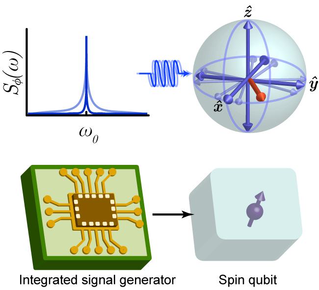
abstract = {As quantum networks expand and are deployed outside research laboratories, a need arises to design and integrate compact control electronics for each memory node. It is essential to understand the performance requirements for such systems, especially concerning tolerable levels of noise, since these specifications dramatically affect a system's design complexity and cost. Here, using an approach that can be easily generalized across quantum-hardware platforms, a case study based on nitrogen-vacancy (NV) centers in diamond is presented. The effects of phase noise and timing jitter in the control system in conjunction are modeled and experimentally verified with the spin qubit's environmental noise. The impact of different phase noise characteristics on the fidelity of dynamical decoupling sequences is also considered. The results demonstrate a procedure to specify design requirements for integrated quantum control signal generators for solid-state spin qubits, depending on their coherence time, intrinsic noise spectrum, and required fidelity.},

keywords = {},

pubstate = {published},

tppubtype = {article}

}

