2023
|
 | Omirzakhov, Kaisarbek; Idjadi, Mohamad Hossein; Huang, Tzu-Yung; Breitweiser, Alex S; Hopper, David A; Bassett, Lee C; Aflatouni, Firooz An Integrated Reconfigurable Spin Control System on 180 nm CMOS for Diamond NV Centers Journal Article IEEE Transactions on Microwave Theory and Techniques, pp. 1-12, 2023. Abstract | Links | BibTeX | Tags: diamond NV center, Quantum Control, spin readout @article{Omirzakhov2023,
title = {An Integrated Reconfigurable Spin Control System on 180 nm CMOS for Diamond NV Centers},
author = {Kaisarbek Omirzakhov and Mohamad Hossein Idjadi and Tzu-Yung Huang and S. Alex Breitweiser and David A. Hopper and Lee C. Bassett and Firooz Aflatouni},
url = {https://ieeexplore.ieee.org/document/10079193/keywords#keywords},
doi = {10.1109/TMTT.2023.3254600},
year = {2023},
date = {2023-03-23},
journal = {IEEE Transactions on Microwave Theory and Techniques},
pages = {1-12},
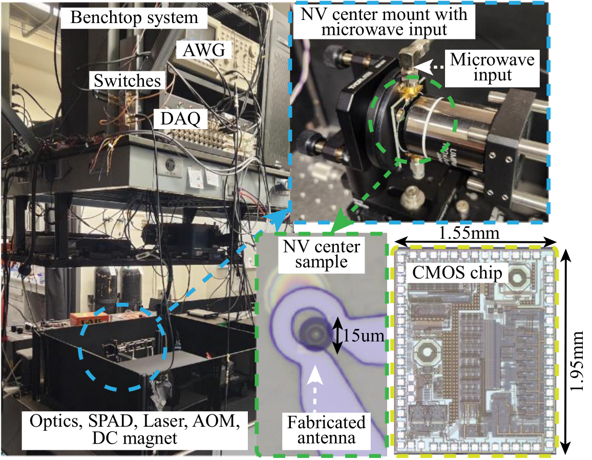
abstract = {Solid-state electron spins are key building blocks for emerging applications in quantum information science, including quantum computers, quantum communication links, and quantum sensors. These solid-state spins are mainly controlled using complex microwave pulse sequences, which are typically generated using benchtop electrical instruments. Integration of the required electronics will enable realization of a scalable low-power and compact optically addressable quantum system. Here, we report an integrated reconfigurable quantum control system, which is used to find electron-spin resonance (ESR) frequency and perform Rabi, Ramsey, and Hahn-echo measurements for a nitrogen-vacancy (NV) center spin qubit in diamond. The chip can be programmed to synthesize an RF signal tunable from 1.6 to 2.6 GHz, which is modulated with a sequence of up to 4098 reconfigurable pulses with a pulse width and pulse-to-pulse delay adjustable from 10 ns to 42 ms and 18 ns to 42 ms, respectively, at a resolution of 2.5 ns. The 180-nm CMOS chip is fabricated within a footprint of 3.02 mm 2 and has a power consumption of 80 mW.},
keywords = {diamond NV center, Quantum Control, spin readout},
pubstate = {published},
tppubtype = {article}
}
Solid-state electron spins are key building blocks for emerging applications in quantum information science, including quantum computers, quantum communication links, and quantum sensors. These solid-state spins are mainly controlled using complex microwave pulse sequences, which are typically generated using benchtop electrical instruments. Integration of the required electronics will enable realization of a scalable low-power and compact optically addressable quantum system. Here, we report an integrated reconfigurable quantum control system, which is used to find electron-spin resonance (ESR) frequency and perform Rabi, Ramsey, and Hahn-echo measurements for a nitrogen-vacancy (NV) center spin qubit in diamond. The chip can be programmed to synthesize an RF signal tunable from 1.6 to 2.6 GHz, which is modulated with a sequence of up to 4098 reconfigurable pulses with a pulse width and pulse-to-pulse delay adjustable from 10 ns to 42 ms and 18 ns to 42 ms, respectively, at a resolution of 2.5 ns. The 180-nm CMOS chip is fabricated within a footprint of 3.02 mm 2 and has a power consumption of 80 mW. |
2020
|
 | Bassett, L C Quantum optics with single spins Book Chapter Mario Agio Irene D’Amico, Rashid Zia Costanza Toninelli (Ed.): 204 , pp. 115-144, IOS Press, 2020, ISBN: 978-1-64368-099-6. Abstract | Links | BibTeX | Tags: Condensed Matter, Quantum Control @inbook{Bassett2019,
title = {Quantum optics with single spins},
author = {L C Bassett},
editor = {Mario Agio, Irene D’Amico, Rashid Zia, Costanza Toninelli},
url = {https://ebooks.iospress.nl/doi/10.3254/ENFI200022
https://arxiv.org/abs/1908.05566},
doi = {10.3254/ENFI200022},
isbn = {978-1-64368-099-6},
year = {2020},
date = {2020-12-16},
volume = {204},
pages = {115-144},
publisher = {IOS Press},
series = {Proceedings of the International School of Physics "Enrico Fermi"},
abstract = {Based on lectures at the 2018 International School of Physics "Enrico Fermi", Course 204: Nanoscale Quantum Optics
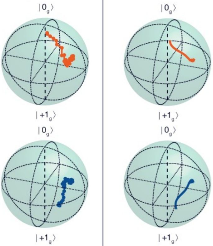
Defects in solids are in many ways analogous to trapped atoms or molecules. They can serve as long-lived quantum memories and efficient light-matter interfaces. As such, they are leading building blocks for long-distance quantum networks and distributed quantum computers. This chapter describes the quantum-mechanical coupling between atom-like spin states and light, using the diamond nitrogen-vacancy (NV) center as a paradigm. We present an overview of the NV center's electronic structure, derive a general picture of coherent light-matter interactions, and describe several methods that can be used to achieve all-optical initialization, quantum-coherent control, and readout of solid-state spins. These techniques can be readily generalized to other defect systems, and they serve as the basis for advanced protocols at the heart of many emerging quantum technologies.},
keywords = {Condensed Matter, Quantum Control},
pubstate = {published},
tppubtype = {inbook}
}
Based on lectures at the 2018 International School of Physics "Enrico Fermi", Course 204: Nanoscale Quantum Optics
Defects in solids are in many ways analogous to trapped atoms or molecules. They can serve as long-lived quantum memories and efficient light-matter interfaces. As such, they are leading building blocks for long-distance quantum networks and distributed quantum computers. This chapter describes the quantum-mechanical coupling between atom-like spin states and light, using the diamond nitrogen-vacancy (NV) center as a paradigm. We present an overview of the NV center's electronic structure, derive a general picture of coherent light-matter interactions, and describe several methods that can be used to achieve all-optical initialization, quantum-coherent control, and readout of solid-state spins. These techniques can be readily generalized to other defect systems, and they serve as the basis for advanced protocols at the heart of many emerging quantum technologies. |
2019
|
 | Poteshman, Abigail N; Tang, Evelyn; Papadopoulos, Lia; Bassett, Danielle S; Bassett, Lee C Network architecture of energy landscapes in mesoscopic quantum systems Journal Article New Journal of Physics, 21 , pp. 123049, 2019. Abstract | Links | BibTeX | Tags: complex quantum systems, network science, Quantum Control, topology @article{Poteshman2019,
title = {Network architecture of energy landscapes in mesoscopic quantum systems},
author = {Abigail N Poteshman and Evelyn Tang and Lia Papadopoulos and Danielle S Bassett and Lee C Bassett},
url = {https://iopscience.iop.org/article/10.1088/1367-2630/ab5c9f
https://arxiv.org/abs/1811.12382},
doi = {10.1088/1367-2630/ab5c9f},
year = {2019},
date = {2019-12-20},
journal = {New Journal of Physics},
volume = {21},
pages = {123049},
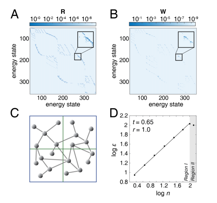
abstract = {Mesoscopic quantum systems exhibit complex many-body quantum phenomena, where interactions between spins and charges give rise to collective modes and topological states. Even simple, non-interacting theories display a rich landscape of energy states --- distinct many-particle configurations connected by spin- and energy-dependent transition rates. The collective energy landscape is difficult to characterize or predict, especially in regimes of frustration where many-body effects create a multiply degenerate landscape. Here we use network science to characterize the complex interconnection patterns of these energy-state transitions. Using an experimentally verified computational model of electronic transport through quantum antidots, we construct networks where nodes represent accessible energy states and edges represent allowed transitions. We then explore how physical changes in currents and voltages are reflected in the network topology. We find that the networks exhibit Rentian scaling, which is characteristic of efficient transportation systems in computer circuitry, neural circuitry, and human mobility, and can be used to measure the interconnection complexity of a network. Remarkably, networks corresponding to points of frustration in quantum transport (due, for example, to spin-blockade effects) exhibit an enhanced topological complexity relative to networks not experiencing frustration. Our results demonstrate that network characterizations of the abstract topological structure of energy landscapes can capture salient properties of quantum transport. More broadly, our approach motivates future efforts to use network science in understanding the dynamics and control of complex quantum systems.},
keywords = {complex quantum systems, network science, Quantum Control, topology},
pubstate = {published},
tppubtype = {article}
}
Mesoscopic quantum systems exhibit complex many-body quantum phenomena, where interactions between spins and charges give rise to collective modes and topological states. Even simple, non-interacting theories display a rich landscape of energy states --- distinct many-particle configurations connected by spin- and energy-dependent transition rates. The collective energy landscape is difficult to characterize or predict, especially in regimes of frustration where many-body effects create a multiply degenerate landscape. Here we use network science to characterize the complex interconnection patterns of these energy-state transitions. Using an experimentally verified computational model of electronic transport through quantum antidots, we construct networks where nodes represent accessible energy states and edges represent allowed transitions. We then explore how physical changes in currents and voltages are reflected in the network topology. We find that the networks exhibit Rentian scaling, which is characteristic of efficient transportation systems in computer circuitry, neural circuitry, and human mobility, and can be used to measure the interconnection complexity of a network. Remarkably, networks corresponding to points of frustration in quantum transport (due, for example, to spin-blockade effects) exhibit an enhanced topological complexity relative to networks not experiencing frustration. Our results demonstrate that network characterizations of the abstract topological structure of energy landscapes can capture salient properties of quantum transport. More broadly, our approach motivates future efforts to use network science in understanding the dynamics and control of complex quantum systems. |
 | Bassett, L C; Alkauskas, A; Exarhos, A L; Fu, K -M C Quantum defects by design Journal Article Nanophotonics, 8 (11), 2019. Abstract | Links | BibTeX | Tags: Nanophotonics, optical sources, point defects, Quantum Control @article{Bassett2019b,
title = {Quantum defects by design},
author = {L. C. Bassett and A. Alkauskas and A. L. Exarhos and K.-M. C. Fu},
url = {https://www.degruyter.com/view/journals/nanoph/8/11/article-p1867.xml},
year = {2019},
date = {2019-10-04},
journal = {Nanophotonics},
volume = {8},
number = {11},
abstract = {Part of Special Issue on Quantum Nanophotonics in Emerging Materials.
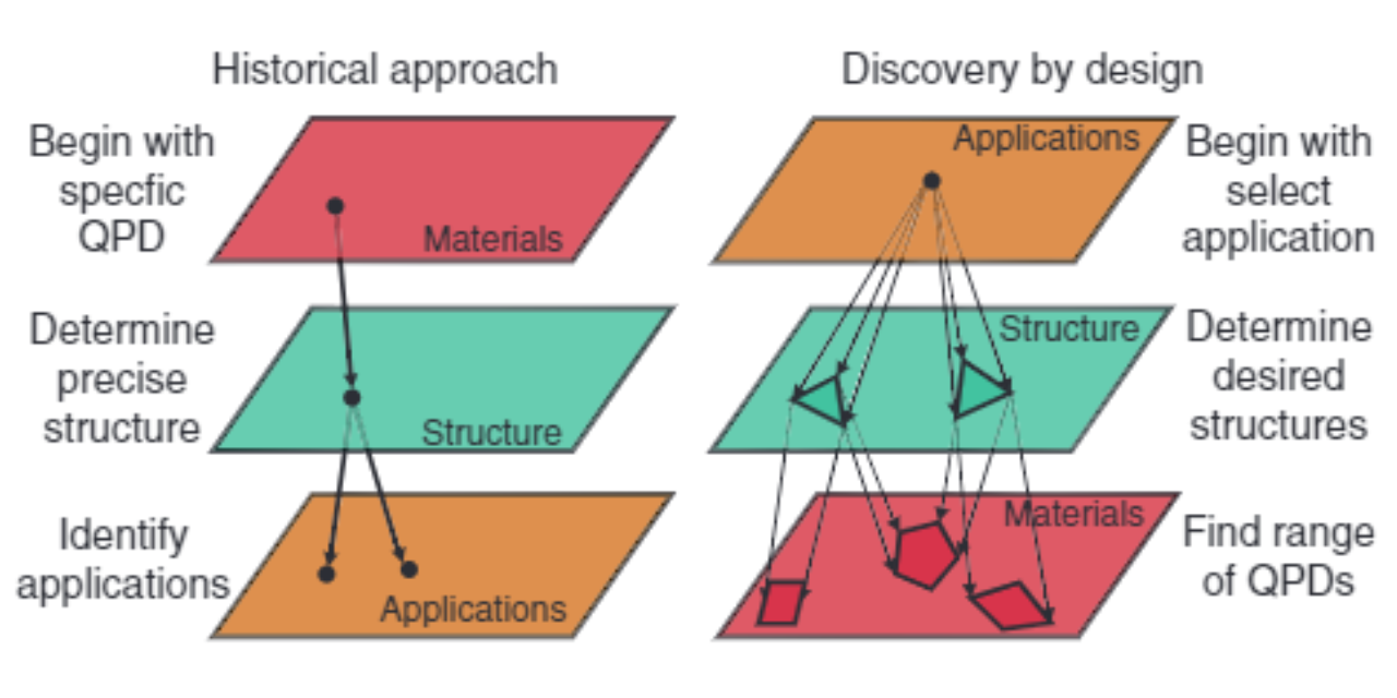
Miniaturization of electronic and opto-electronic semiconductor devices has been happening ever since the first such devices appeared. Eventually, one can envision a device that is composed of just a few atoms. As these atoms ideally should not float in free space, but should be embedded in a solid-state matrix, this naturally brings one to the concept of a point defect (an impurity atom or complex of atoms) as the ultimate electronic or opto-electronic device. At such tiny length scales the behavior of physical systems is governed by the laws of quantum mechanics. Therefore, it is no surprise that an increasing number of point defects are being considered as building blocks for various applications in the field of quantum information science; more specifically, in quantum sensing, quantum communication, and quantum computing [1], [2], [3], [4]. We refer to these desirable defects as quantum point defects (QPDs). Prominent examples include the nitrogen-vacancy (NV) center in diamond, the silicon-vacancy (SiV) center in diamond, the divacancy in silicon carbide, and rare-earth impurities in complex oxides.},
keywords = {Nanophotonics, optical sources, point defects, Quantum Control},
pubstate = {published},
tppubtype = {article}
}
Part of Special Issue on Quantum Nanophotonics in Emerging Materials.
Miniaturization of electronic and opto-electronic semiconductor devices has been happening ever since the first such devices appeared. Eventually, one can envision a device that is composed of just a few atoms. As these atoms ideally should not float in free space, but should be embedded in a solid-state matrix, this naturally brings one to the concept of a point defect (an impurity atom or complex of atoms) as the ultimate electronic or opto-electronic device. At such tiny length scales the behavior of physical systems is governed by the laws of quantum mechanics. Therefore, it is no surprise that an increasing number of point defects are being considered as building blocks for various applications in the field of quantum information science; more specifically, in quantum sensing, quantum communication, and quantum computing [1], [2], [3], [4]. We refer to these desirable defects as quantum point defects (QPDs). Prominent examples include the nitrogen-vacancy (NV) center in diamond, the silicon-vacancy (SiV) center in diamond, the divacancy in silicon carbide, and rare-earth impurities in complex oxides. |